Specifications
Include DB->SB thru 96 pin connector (fig 35, pg 44 User Guide)
Quick USB: back of SB or Host PC Interface Board
Introduction
Need intro?
(Describe how the various elements interface with each other. Use simple diagrams from Framework, source code and hardware schematics. Example: Revisit Framework figure 5, pg 12 with specification details of clock frequency, protocol lines, etc.)
Timing Signals
Introduction
The system level timing signals are shown in Fig. 10. There are two timing signals–the System Clock that is an 80 MHz clock signal, and the Time Slice Boundary that defines the beginning of a Time Slice. The firmware will support both “short” and “long” event words. In “short” mode, the Time Slice Boundary is generated every eight System Clock cycles (100 ns). In “long” mode, it is generated every sixteen System Clock cycles (200 ns). The choice creates a tradeoff–in “short” mode the dead time is a factor of two shorter, but the number of bits per event word is also a factor of two smaller (32-bit verses 64-bit).
The general concept is that the system divides time into small, fixed length Time Slices. During one Time Slice, each of the boards in a Standard System that output singles event words (i.e., DB, CI-1, and MB-1) can pass four singles event words. Thus, the maximum singles rate seen at the CI-1 output of each Detector Unit is 4 singles event words per Time Slice, or approximately 40 million “short” singles event words per second. Thus, 32 singles event words (four for each of the eight CI-1) enter the Coincidence Unit per Time Slice, or approximately 320 million “short” singles event words per second. In a Standard System, there are 8 Detector Units with 28 possible Detector Unit - Detector Unit combinations. So theoretically the Coincidence Unit can identify 448 coincident events per Time Slice (16 for each of the 28 Detector Unit-Detector Unit combinations), corresponding to 4.48 billion coincidence event words per second. In practice, the maximum event rate is limited by the transfer rate between the Coincidence Unit and the Host PC, which is considerably slower.
(Make sure rest of document is consistent with the above paragraph)
Time Slice Boundary
The rising edge of the Time Slice Boundary defines the beginning of a Time Slice. The width of the pulse is one System Clock cycle, and the period is eight System Clock cycles . In general, it is generated on the Support Board in the Coincidence Unit (although it can be generated on the Support Board in a Detector Unit such as in the Small System), and then buffered through the rest of the system. Propagation delays will introduce skewing; therefore each FPGA that outputs data also outputs a copy of the Time Slice Boundary that is synchronized with its output data signals. The rising edge of the Time Slice is also offset by 3.125ns so that it happens before the rising edge of the Clock cycle. This way, the Time Slice is not missed.
Note
There is a 3.125ns difference between clock and slice rising edges. Slice precedes clock. As can be in Fig. 10.
Time Slice
As previously mentioned, the system divides time into small, fixed length Time Slices (100-200 ns or 8-16 clocks). All individual data processing operations must occur within a single Time Slice, which implies that only singles event words that occur in the same Time Slice can be combined to form a coincident event. While it can take significantly longer than one Time Slice to fully process a single event, the system is pipelined so that the processing is divided into smaller operations that each can be completed in a single Time Slice. It takes one Time Slice to transfer a singles event word.
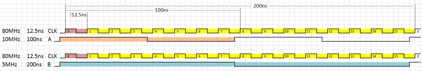
Fig. 10 System level timing signals. Slices A and B are 3.125ns early.
Currently, the time slice is set when the firmware is compiled. There is a variable g_slice_div that is either 0 or 1 which corresponds to a division by 8 or a division by 16. The former is for the 100ns time slice, and the latter is for the 200ns time slice as can be seen in Fig. 10. In the future, the time slice will be runtime user configurable so that the firmware does not need to be compiled every time the user wants to change the time slice.
Clocking
The clock signal flow of the OpenPET system in general is illustrated with Fig. 11. There are four clock domains that are explained in more detail below.
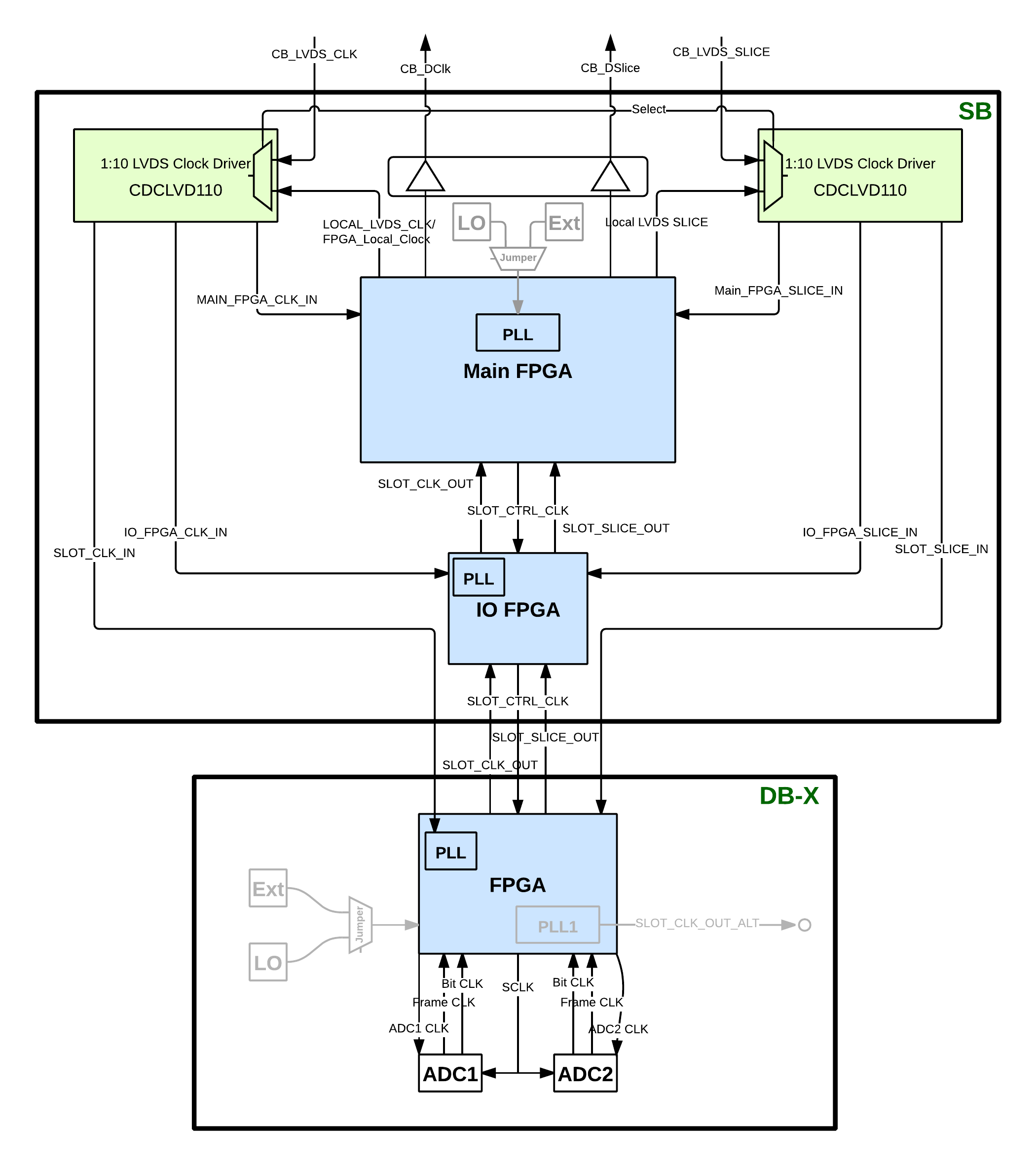
Fig. 11 Clock distribution diagram.
System Clock
The System Clock is an 80MHz clock. In general, it is generated by a local oscillator (crystal) or external signal on the Support Board in the Coincidence Unit (although it can be generated on the Support Board in a Detector Unit such as in the Small System), and then buffered through the rest of the system. Propagation delays will introduce skewing, therefore each FPGA that outputs data also outputs a copy of the System Clock that is synchronized with its output data signals. In general, each board in the system regenerates the clock using a phase-locked loop (PLL) in order to maintain signal quality and to minimize phase drift. The System Clock signal also goes to the NIOS II processor and other components connected to NIOS II.
ADC Clock
The ADC Clock is a 40MHz clock. This signal is derived from the 80MHz System Clock signal. An output from the Coincidence Unit (or Detector Unit) PLL goes to a clock distributor that takes the 80MHz signal and creates ten duplicate signals. Eight of these signals go to the Detector Boards, one signal per board. Each Detector Board takes the 80MHz signal and passes it through a PLL on its Main FPGA in order to maintain signal quality and to minimize phase drift. One of the PLL outputs is 40MHz and this is the ADC clock. It is used by the ADC on the board, and for signal processing of incoming data. It is also used for backplane transfer.
QuickUSB Clock
The QuickUSB clock is a 30MHz clock. It is essentially derived from the System Clock signal. It is an output of the PLL on the Main FPGA of the Support Board in the Coincidence Unit (or Detector Unit for a Small System). QuickUSB is used to send and receive data.
Ethernet Clock
The Ethernet Clock is not in use yet, but will be a 125MHz clock. An 80MHz signal from the PLL on the Main FPGA of the Support Board in the Coincidence Unit (or Detector Unit for a Small System) is sent to an additional PLL on the same Main FPGA. One of the outputs is a 125MHz signal that is sent to the PHY transceiver. Ethernet is used to send and receive data.
Small System Example
To describe the clock signals in more detail, we will use a small system example. In a small system, the support board on the CDUC connects to all the detector boards (Fig. 12).
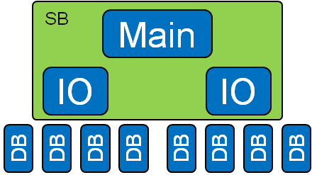
Fig. 12 Small system block diagram.
The clock signal schematic is shown in Fig. 11. For the purpose of this explanation and example, the support board is on the CDUC and is connected to eight identical detector boards labeled DB-X in the figure. Since the CDUC is the top node of the system, any incoming and outgoing clock and slice signals at the top of the support board can be ignored.
On the support board, the clock signal that feeds into the Main FPGA PLL can come from two different places. Either a local oscillator (crystal) at 80MHz or an external clock connected through an SMA cable. The user defines which is used based on jumper placement. For the small system, the clock defaults to the local oscillator at 80MHz. This PLL’s outputs feed the rest of the system. One 80MHz output travels to the NIOS processor and the U30 clock distributor (left side). The time slices are also generated with this PLL, both the 5MHz (200ns) and the 10MHz (100ns). The time slice signal goes to the U29 clock distributor (right side). Each time slice has its own PLL output. There is additionally a 30MHz output that goes to the QuickUSB. (There is a new Ethernet option which takes a 80MHz signal from the NIOS line and feeds another PLL. This PLL then outputs a 125MHz signal to a Marvell Ethernet PHY chip.)
For the clock signal (left side of Fig. 11), the U30 clock distributor takes the 80MHz input from the PLL and duplicates it ten times. There is a voltage source connected in order to accomplish this. One output is a feedback to the PLL, one splits and goes to both IOs, and each of the other eight go to a detector board.
For the time slice signal (right side of Fig. 11), the time slice signal (5MHz or 10MHz) travels from the PLL to the U29 clock distributor. This clock distributor also takes the input and duplicates it ten times. One output is a feedback to the PLL, one splits and goes to both IOs, and each of the other eight go to a detector board.
On the detector board, there are clock and slice inputs and outputs. The clock coming in is a 80MHz going into the PLL. The PLL has one output at 80MHz going to the NIOS. Another output goes to the ADC clocks at 40MHz which then go to ADC1 and ADC2.
From the Main FPGA, the SPI sets a control clock to the IO FPGA. This clock is 1MHz from the NIOS processor.
Power
Crate
A Support Crate (Fig. 13) consists of a standard 12-slot VME chassis that accommodates 6U x 160 mm boards, a custom Support Board backplane, power supplies, cooling fans, and appropriate boards plugged into slots 9-11 (Figure 2). Some minor assembly is required for the Support Crate; see the OpenPET User Guide Section 4.2 for detailed assembly instructions.
Elma Electronic Inc. supplies the OpenPET crate chassis installed with power supplies and cooling fans. It is an Elma type 12, 19” rack-mount enclosure with a 7U height. It includes a 740W Vicor power supply with +5 V at 40 A, -5 V at 40 A, +3.3 V at 80 A, +12 V at 6A, and ground outputs. The complete OpenPET chassis specifications are available on at http://openpet.lbl.gov/downloads/hardware/.
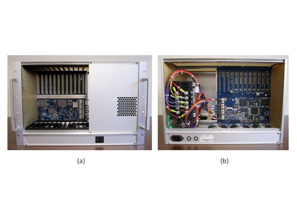
Fig. 13 The assembled OpenPET Support Crate viewed from the (a) front and (b) back.
Support Board
Introduction
In an OpenPET Support Crate, the custom Support Board is mounted as a backplane on a standard 12-slot VME chassis that accommodates 6U boards. This Support Board primarily plays two roles, depending on the firmware. In a Detector Unit for a standard- or large-sized system, the Support Board is loaded with detection firmware and acts as a Detector Unit Controller (SB-DUC in Figure 6). In a Coincidence Unit for a standard- or large-sized system, the Support Board is loaded with coincidence firmware and acts as a Coincidence Unit Controller (SB-CUC in Figure 6).
The Support Board also plays a third role for the special case of a small system when it is configured as a Coincidence Detector Unit Controller (CDUC), which interfaces with the detector boards and performs coincidence functions. Basically the CDUC performs the functions of both the CUC and DUC.
Repository
There are five directories in the SupportBoard repository that are outlined below.
doc
This directory contains the documentation for hardware, firmware, and embedded software.
fw
This directory contains the Altera firmware projects for the 3 FPGAs on the support board. In order to build the firmware as well as the embedded software that runs on the NIOS II CPU, the user should follow the simple commands below:
Building the firmware and flash images for the Support Board:
Windows x86 and x64 OSs:
- Open your file browser i.e. Explorer and go to ./scripts directory
- Double click on ‘buildFirmware.bat’ to launch firmware building flow.
- By default CDUC firmware is built. If you like to build another firmware edit ‘buildFirmware.bat’ and change CDUC to CUC or whatever you like.
- If you don’t what to edit the bat file. Open a Command Prompt and type alt_win.cmd buildFirmware.sh CUC
- Follow the prompts.
Unix x86 and x64 POSIX OSs:
- Open a terminal and navigate to ./scripts
- execute buildFirmware.sh by typing ./buildFirmware.sh
- By default CDUC firmware is built. If you like to built a firmware for another controller type ./buildFirmware.sh CUC
- Follow the prompts.
Note
It is possible to program the flash on the Main FPGA using the flashboard script. All the following compiled images will be stored in ./scripts/bin
- IO 1-4 SOF image
- IO 5-8 SOF image
- Main FPGA SOF image
- main.hex is the ELF program that runs on the NIOS II CPU in the Main FPGA
- supportboard.jic is the flash image which contains the four files listed above
To flash on Windows just double click on flashboard.bat. If you need to change the cable then edit the bat file and change the cable index number.
On Unix, just run ./flashboard.sh or ./flashboard.sh 2 where 2 is the USB blaster cable index.
hw
This directory contains the PCB schematic and layout files using Orcad tools. It also has the bill of materials (BOM) for your convenience.
scripts
sw
This directory contains the embedded software which runs on the soft CPU core (NIOS II) in the Main FPGA. In order to build the ELF file associated with this project, one has to build the Qsys and Quartus projects in the firmware directory first. Follow the directions listed under “fw” section to build the embedded software using buildFirmware script.
Support Board with Detection Firmware
In an OpenPET Support Crate, the custom Support Board is mounted as a backplane on a standard 12-slot VME chassis that accommodates 6U boards. This Support Board primarily plays two roles, depending on the firmware. In a Detector Unit for a standard- or large-sized system, the Support Board is loaded with detection firmware and acts as a Detector Unit Controller (SB-DUC in Figure 6). In a Coincidence Unit for a standard- or large-sized system, the Support Board is loaded with coincidence firmware and acts as a Coincidence Unit Controller (SB-CUC in Figure 6).
The Support Board also plays a third role for the special case of a small system when it is configured as a Coincidence Detector Unit Controller (CDUC), which interfaces with the detector boards and performs coincidence functions. Basically the CDUC performs the functions of both the CUC and DUC.
In summary, digital IO is performed on the Support Board in a Detector Unit or Coincidence Unit with the following specifications (Fig. 14):
- Through Main FPGA:
- 16 bits digital IO (4 bits direction control)
- 10 Bits LED bar
- Two logic analyzer connectors (16+1 bits each)
- Through IO FPGA 1:
- 16 bits digital IO (4 bits direction control)
- 10 Bits LED bar
- One logic analyzer connector (16+1 bits each)
- Through IO FPGA 2:
- 16 bits digital IO (4 bits direction control)
- 10 Bits LED bar
- One logic analyzer connector (16+1 bits each)
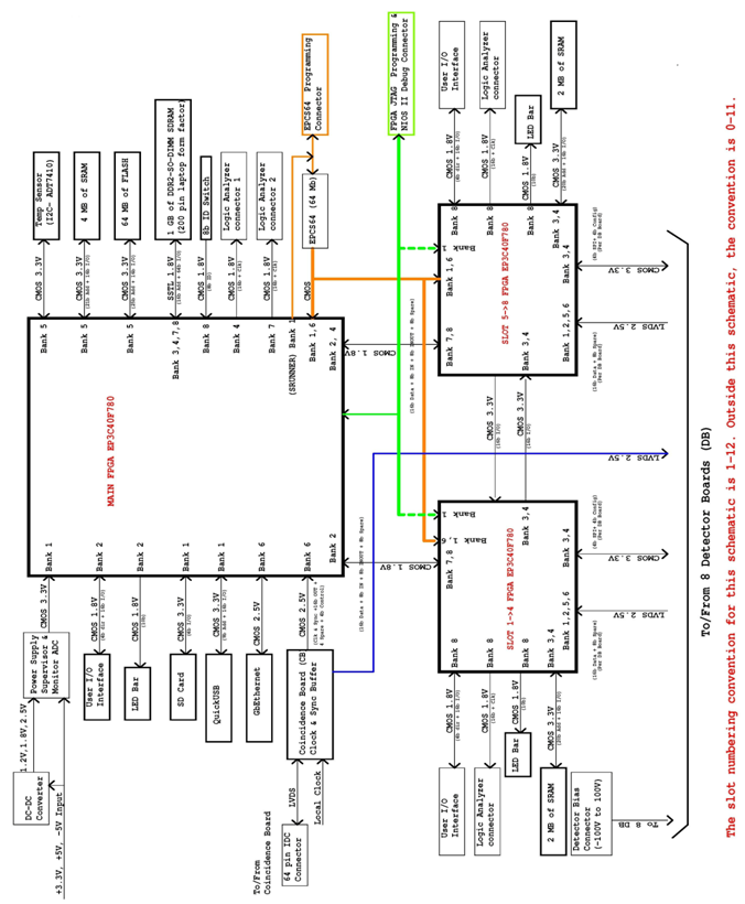
Fig. 14 Support Board overview schematic diagram (Page 1 Title Block Diagram).
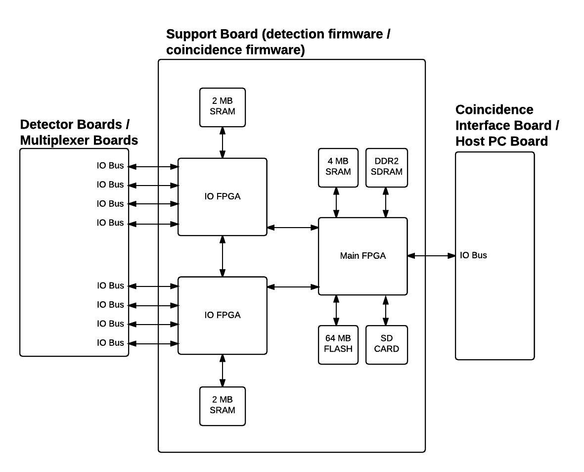
Fig. 15 Schematic of the Support Board, which is loaded with either detection firmware (when used in a Detector Unit) or coincidence firmware (when used in a Coincident Unit).
IO FPGAs
There are two slave IO FPGAs on the Support Board. These act primarily as a multiplexer for singles events, each taking up to 16 individual singles events that it can receive in a single time frame and passing up to 4 of them to the Main FPGA. Obviously, there is some possibility for data loss, and the multiplexing algorithm is designed to ensure that this loss is unbiased. Each IO FPGA also serves as a fan-in and fan-out for communication between the Main FPGA and the individual Detector Boards, and the two IO FPGAs can communicate with each other.
The digital signals between each IO FPGA and the Main FPGA are identical to the standard OpenPET Bus IO signals (Fig. 16): lines for the clock and Time Slice Boundary (both directions), 4 control lines, 4 FPGA programming lines, 16 event data lines, and eight user-definable data lines. There are also 32 user-definable digital lines between the two IO FPGAs, 16 sending data in each direction.
Main FPGA
A single physical Main FPGA performs the logical functions of both the master FPGA and the support microprocessor. Its FPGA-like functions are mostly limited to passing events from the IO FPGAs to the Coincidence Interface Board (providing multiplexing, if necessary).
Some of the logic blocks in the Main FPGA can be programmed using Nios II to be identical to microprocessor hardware, which then runs executable files programmed in C. This support microprocessor receives high-level commands from the Host PC via USB (or Gigabit Ethernet or Fiber-Optics), and then interprets and executes these commands. It is responsible for loading all the programs into the IO FPGAs and DB FPGA, as well as the contents of all the support memory, detector memory, and all other registers that are on the DB and SB. It also monitors the event stream and can insert diagnostic information (such as event rates) into the event stream or provide this information directly to the Host PC. Whenever possible, calibration routines are also performed on the support
Support Memory
There are multiple forms of memory on the Support Board, as shown in Fig. 14. The SRAM is accessed by the FPGA and provides its output within 1 clock cycle of being addressed so it is both reasonably fast and deterministic, which greatly simplifies incorporating it within FPGA algorithms. However, the SRAM capacity is fairly small. Thus, the Main FPGA is connected to 4 MB of SRAM and each of the IO FPGAs is connected to 2 MB of SRAM, for a total of 8 MB of SRAM on each Support Board. This memory is typically used to store look-up tables that apply real time calibration and corrections to the event data.
As the Main FPGA also emulates a microprocessor, RAM memory and disk storage are also necessary for it to function effectively. The RAM memory is provided via up to 1 GB of RAM that can be plugged into a DDR2 SDRAM connector (identical to that typically found in laptop computers). The disk storage is provided by a SD card (identical to that found in digital cameras) that is plugged into a SD card slot, when users desire disk storage that can be easily removed. Otherwise, standard disk storage is provided by a 64 MB FLASH memory chip that is connected to the Main FPG, in order to store the FPGA firmware needed for DB FPGAs, contents of all the support SRAM memory, detector memory, and all other registers that are on the DB and SB. This information can also be stored in the on-board EPCS memory, which is where it resides in the initial release.
In summary, the Support Board has the following memory available, as shown in Fig. 14:
- Through Main FPGA:
- Flash memory
- EPCS64 flash memory
- 64 MB flash memory
- RAM
- 4 MB SRAM
- 1 GB DDR2-SO-DIMM SDRAM
- Through IO FPGA 1:
- RAM
- 2 MB SRAM
- Through IO FPGA 2:
- RAM
- 2 MB SRAM
Clock Conditioning
The clock-conditioning block consists of a PLL (phase-locked loop) that regenerates the system clock signal from the Support Board in a Coincidence Unit and passes it to the Support Board FPGAs in a Detector Unit and then to the Detector Boards. The block also includes space for a local clock oscillator (i.e., LO in Fig. 11), which is used to provide the system clock when the system is being used without a Coincidence Unit (i.e., when the support microprocessor passes events directly to the host computer).
Connectors
The connector that is soldered onto the SB in order to connect to a single DB (slot 0-7) is a 96 pin female connector, press fit for a 0.125” thick board, Vector Electronics RE96FSP (Digi-Key part number V1240-ND). This connector is also used for slots 8-10, and two of these connectors are used for slot 11. See below for more details.
Miscellaneous Devices
The Support Board also contains signals for miscellaneous devices, including temperature sensors, two RS232 interfaces, and power monitor.
(Add description of Slots 0-11, like the User Guide? Or describe elsewhere?)
Support Board with Coincidence Firmware
In a Coincidence Unit, the Support Board acts as a Coincidence Unit Controller (SB-CUC) when it is loaded with coincidence firmware, as shown in Figure 6. It also provides control and power for the Multiplexer Boards that are located in slots 0-7.
In the general data flow, singles event words are passed through a Coincidence Interface Board to a Multiplexer Board, which can provide a further layer of multiplexing for singles event words, if necessary. These multiplexed singles event words are then passed to the Support Board with coincidence firmware, which searches through the singles event words from multiple (up to eight) MBs for pairs that are in time coincidence and then forms coincidence event words. These coincidence event words are then passed to the Host PC through the Host PC Interface Board. Optionally, the Coincidence Unit Controller can act as a multiplexer and forward unaltered singles event words to the Host PC.
When the Support Board acts as a Coincidence Unit Controller, the role of the three FPGAs is similar to that described above. Each IO FPGA acts as a multiplexer for singles event words, taking up to 16 individual singles events from MBs and passing up to four of them to the Main FPGA, using a multiplexing algorithm that ensures unbiased loss. The Main FPGA acts as both a master FPGA and a support microprocessor. As a master FPGA, it primarily passes events from the IO FPGA to the Host PC Interface Board. As a support microprocessor, Nios II is used to program logical blocks in the FPGA to run executable files programmed in C. For instance, the Main FPGA is used to identify and form coincident event words.
High-level commands are sent via USB (or Ethernet or Fiber-Optic) from the Host PC to the Coincidence Unit. The NIOS II microprocessor is not connected directly to these communication interfaces. Instead, the NIOS II microprocessor talks to the communication interfaces through the register array implemented in the Main FPGAs.
Support Board with Detection & Coincidence Firmware
In the special case of a Small System, the Support Board is also capable of identifying coincident pairs of singles event words, formatting them into coincidence event format, and passing them to the support microprocessor (Main FPGA), which then passes them to the Host PC. Thus it can act as a full-featured PET data acquisition system, albeit with a limited number of input channels and output event rate capability. It can also be programmed to multiplex singles events and pass them to the Host PC.
Detector Board
Introduction
The overall purpose of the Detector Board is to process the analog inputs from the detector modules in the system and convert them into singles event words. Generally, this requires determining the energy, interaction position, and arrival time associated with a single gamma ray interaction that occurs in the detector module, as well as applying as many corrections as possible before the associated singles event word is generated.
In order to process an analog input signal, the Detector Board contains an analog front-end circuit with amplification and filtering to reduce the noise and bandwidth of the signal. The processed analog signal is subsequently digitized by an analog-to-digital converter (ADC) to capture the processed analog signal. For systems that require good timing resolution such as PET, additional circuitry may be implemented in the front end to split the analog input signal into a fast timing path where the signal is amplified with a high-bandwidth amplifier. The amplified signal is then triggered by a fast leading edge discriminator to create a timing pulse for the signal arrival, which is time stamped by a time-to-digital converter (TDC) implemented inside the FPGA.
The back end of the Detector Board primarily consists of an FPGA and static random access memory (SRAM). The FPGA processes the digitized signals from the ADCs and, if necessary, combines information from multiple channels to compute the deposited energy, the interaction position, and the event time. Appropriate calibration correction factors that are stored in the SRAM can also be applied to the data. The computed information are formatted into a singles event word and then transferred to the Support Board (i.e., SB-DUC) via the standard OpenPET Bus IO, as described in Bus IO. In addition, the firmware for the FPGA is loaded into the Detector Board by the Support Board via the standard Bus IO. Different firmware can be loaded into the DB FPGA to perform tasks other than event processing, such as debugging, testing, and calibration.
Bus IO
The Bus IO connecting the Detector Board to the Support Board (SB-DUC) is shown schematically in Fig. 16. The bus is divided into several blocks.
One block provides the timing signals using 4 LVDS differential pairs. There are two fundamental timing signals - an 80 MHz System Clock signal generated on the Support Board and a Time Slice Boundary signal that defines the beginning of a Time Slice. The Support Board sends a copy of these System Clock (CLK) and Time Slice Boundary (SLICE) signals, which are used to clock data from the Support Board to the Detector Board. Because there is propagation delay within the Detector Board, another copy of the System Clock and Time Slice Boundary signals (that is produced by the DB) is used to clock data from the Detector Board to the Support Board. In the OpenPET architecture, the system divides time into small, fixed time slices of either 100 ns (8 clocks) or 200 ns (16 clocks). Alternatively, custom time slices can be designed by modification of the firmware, if needed.
A second block defines 4 LVTTL single ended lines to control data between the DB and SB. OpenPET uses a custom serial digital bus protocol comprised of a Clock line (CTRL_CLK), Data In line (CTRL_DI), Data Out line (CTRL_DO), and Chip Selection line (CTRL_CS). However, the Chip Selection line is not utilized in the current protocol. Alternatively, these control lines can be configured to support standard digital serial protocols such as I2C or SPI.
A third block in the Bus IO provides 4 LVTTL single ended lines to program the FPGA on the Detector Board using serial protocols, which are generated by the Support Board. These FPGA programming lines are nCONFIG, DCLK, DATA0, and CONF_DONE.
A fourth block provides 16 LVDS differential pairs (grouped into 4 sets of 4 LVDS differential pairs) to transfer singles event words from the DB to SB. All individual operations must occur within a single time slice, which implies that only singles event words that occur in the same time slice can be combined to form a coincident event. A singles event word can be either a 32-bit word (100 ns time slice) or 64-bit word (200 ns time slice). Since it can take significantly longer than a single time slice to fully process a singles event, the system is pipelined so that the processing is divided into smaller steps that each can be completed in a single time slice. During one time slice, each set of 4 LVDS differential pairs can pass one singles event word (i.e. maximum of 4 singles event words per time slice). Thus, the maximum singles event rate that can be transferred out of each Detector Board is 40 million events per second.
Another block provides 8 spare LVDS differential pairs between the DB and SB for users to pass any information between these two boards.
The final block in the BUS IO supplies power to the Detector Board. Specifically, the Support Board supplies +5 V, +3.3 V, -5 V, and ground.
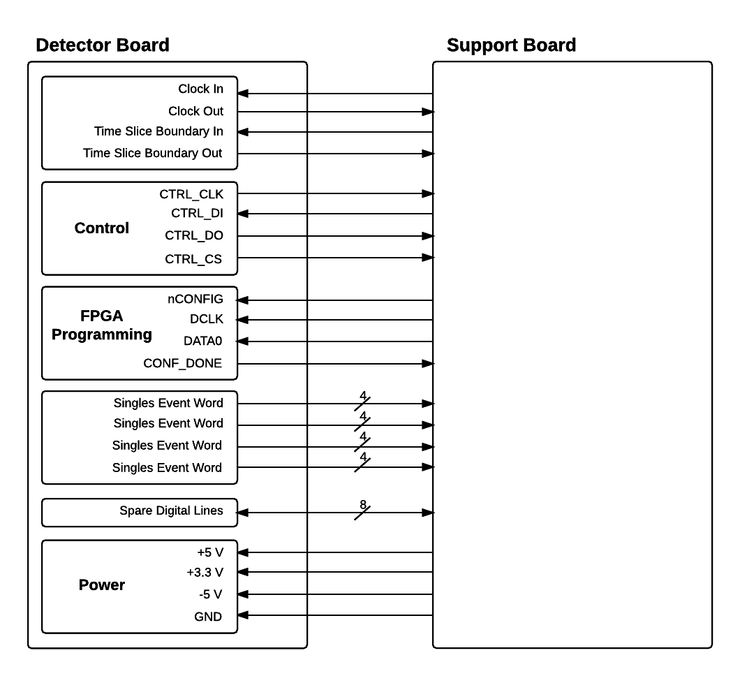
Fig. 16 Diagram of the BUS IO.
16-Channel Detector Board
Fig. 17 shows the block diagram of the 16-channel Detector Board and Fig. 18 shows a photograph. This Detector Board accepts up to 16 analog input signals, each of which is processed independently. The analog input signal is required to be negative polarity, ground referenced. The input analog signal is terminated with 50 ohms, and then split into two processing chains: an energy chain and a timing chain.
The processing circuit for one channel is shown in Fig. 19. The input stage accepts voltages between -0.8 V to 0 V. The input voltage can be attenuated to fall within the acceptable range by changing the attenuation resistor values on the energy chain. Only the signal on the energy chain needs to be attenuated because the range of the input voltage is limited by the dynamic range of the ADC. In addition, there are 8 external differential LVDS IO pairs that can be used to interface to the DB FPGA. The flexibility of these digital IO will allow any digital inputs and/or outputs to be applied to the Detector Board.
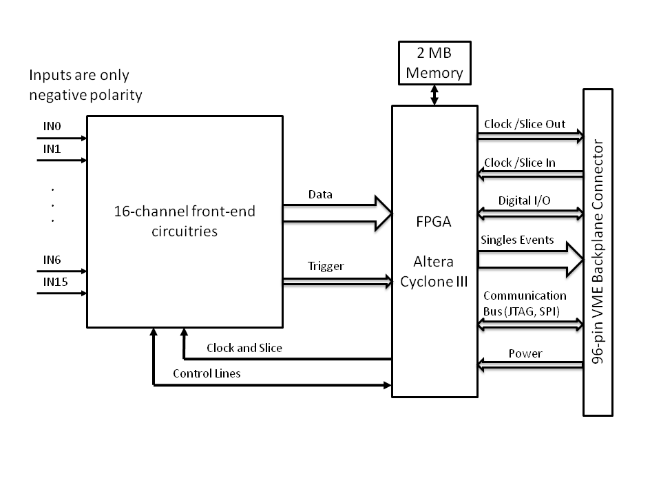
Fig. 17 Block diagram of the 16-channel Detector Board. (Make new version. Replace clock, power, etc lines from the FPGA to 96-pin as BUS IO – i.e. already shown in Fig 12. )
On the energy chain, the input signal is amplified (OPA2694), and then split into an anti-aliasing filter (LTC6605-7) with a cut-off frequency at 7 MHz and a comparator (MAX964). The filtered signal is sent to a 12-bit ADC (ADS5282) that can digitize the signal at a sampling rate from 10 MSPS to 65 MSPS, with a typical sampling rate of 40 MSPS. Each channel of the ADC also has a programmable digital gain from 0 dB to 12 dB. A trigger is generated by the comparator and sent to the FPGA.
On the timing chain, the input signal is amplified with an x10 high-bandwidth (1.8 GHz) amplifier (THS4303) and then sent to a fast comparator (MAX9602) with low propagation delay dispersion (~30 ps) to trigger on the leading edge of the analog signal. We have selected a leading edge discriminator, since several groups have reported that a leading edge discriminator has equivalent or better performance than a constant fraction discriminator (although sometimes requiring amplitude correction for time walk). The generated timing pulse from the comparator is then sent to the DB FPGA, where a TDC is implemented to determine the time stamp of the arrival time of the timing signal.
Further details can be seen on the 16-channel Detector Board schematic shown in Fig. 20 and available on the OpenPET hardware page (log-in required)
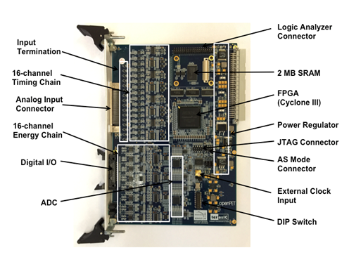
Fig. 18 Photograph of the 16-channel Detector Board.
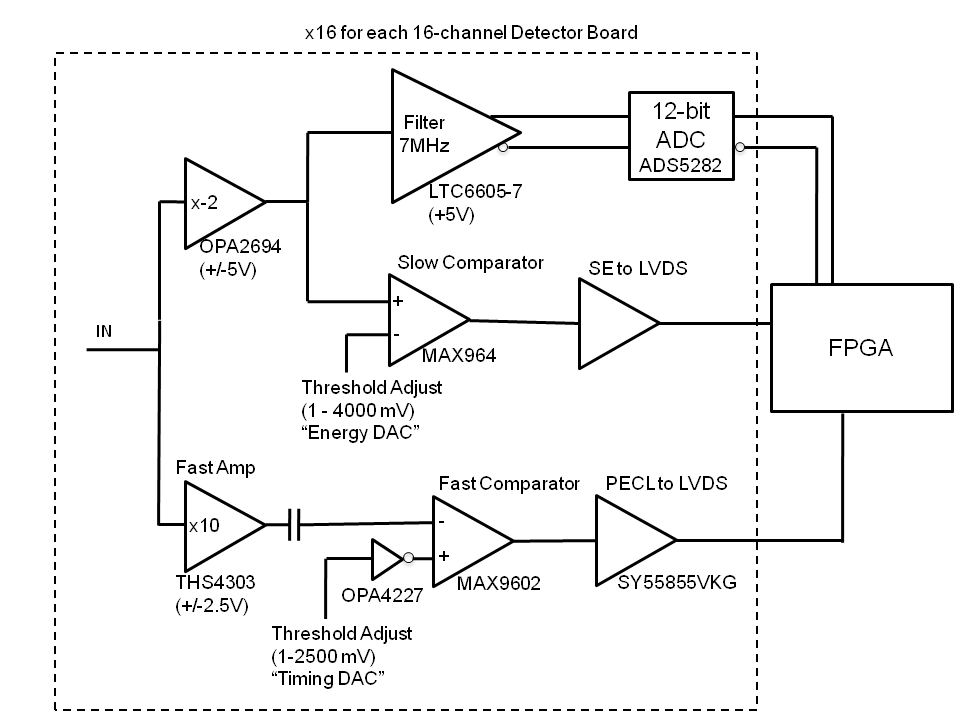
Fig. 19 Block diagram of the front-end circuitries of one channel of the 16-channel Detector Board.
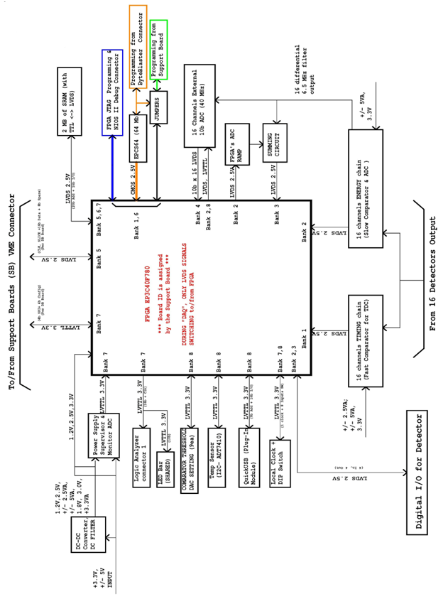
Fig. 20 16-channel Detector Board overview schematic diagram (Title Block Diagram).
Repository
This describes the directories and build instructions for the DetectorBoard16ChLBNL repository.
doc
This directory contains the documentation for hardware, firmware, and embedded software.
fw
This directory contains the Altera firmware projects for the FPGA on the detector board. In order to build the firmware and flash images, the user should follow the simple commands below:
Windows x86 and x64 OSs:
- Open your file browser (i.e., Explorer) and go to ./scripts directory
- Double click on ‘buildFirmware.bat’ to launch firmware building flow.
- By default DB firmware is built. If you like to build another firmware edit ‘buildFirmware.bat’ and change DB to MB or whatever you like.
- If you don’t what to edit the bat file. Open a Command Prompt and type alt_win.cmd buildFirmware.sh MB
- Follow the prompts.
Unix x86 and x64 POSIX OSs:
- Open a terminal and navigate to ./scripts
- Execute buildFirmware.sh by typing ./buildFirmware.sh
- By default DB firmware is built. If you want to build a firmware for another board, type ./buildFirmware.sh DB
- Follow the prompts.
Note
It is possible to program the flash on the FPGA using the flashBoard script. The user should first program the Support Board’s flash and reboot the chassis before programming the detector board.
On Windows, just double click on flashboard.bat. If you need to change the cable, then edit the bat file and change the cable index number.
On Unix, just run ./flashboard.sh or ./flashboard.sh 2 where 2 is the USB blaster cable index.
hw
This directory contains the PCB schematic and layout files using Orcad tools. It also has the bill of materials (BOM) for your convenience.
sw
This directory contains the embedded software which runs on the soft CPU core (NIOS II). In order to build the ELF file associated with this project, one has to build the Qsys and Quartus projects in the firmware directory first. Follow the directions listed under “fw” section to build the embedded software using buildFirmware script.
Coincident Interface & Multiplexor Boards (CI-1 & MB-1)
Host PC Interface Board
See Host PC Interface Board Schematic
Repository
This describes the directories and build instructions for the HostPC repository.
sw
This directory contains software which runs on the Host PC to interface with OpenPET electronics. The following list explains some of the files in this directory.
- ./dist/openpet/openpet.exe: OpenPET command-line utility for Windows x64.
- openpet.py: OpenPET command-line utility source code (cross platform).
- OpenPETlib.py: OpenPET python Library (cross platform).
- QuickUSB.py: QuickUSB library (Developed by Bitwise).
- ctrl_scope_example_simple_DEV.py: A simple example python script to configure and acquire scope data from an OpenPET system.
- ctrl_scope_example_intermediate_DEV.py: An intermediate example python script to configure and acquire scope data from an OpenPET system.
- ctrl_scope_example_advanced_DEV.py: An advanced example python script to configure and acquire scope data from an OpenPET system.
- plot.py: Plots scope data using Matplotlib.
- tdc.py: Plots the tdc values for two channels.
- ctrl_scope_example_simple.cmd: A simple example Windows Batch script wrapper to configure and acquire scope data using openpet.exe.
- README.netmap: Instructions to setup high-speed ethernet acquisition i.e., 992 Mbps
Build Instructions
Windows x64 executable:
If you just want to use the executable you don’t need to continue reading. Just run .../dist/openpet/openpet.exe from your program or wrapper and enjoy the goodness.
Required software to run python scripts (not openpet.exe executable):
- Python 2.7.x (not Python 3.x branch)
- QuickUSB library 2.15.2
- Numpy 1.9+
- Matplotlib 1.4+ (for plotting data)
Installing required software to run python scripts (not openpet.exe executable):
On Windows:
Are you running a 64-bit or a 32-bit Windows? Take a note of that. Typically win32 means 32-bits and amd64 means 64-bit.
Go to https://www.python.org/downloads/windows/ and download the latest 2.7.* branch of Python
Configure the Python installer to add python to your PATH environment variables or do it manually by appending C:Python27;C:Python27Scripts to your PATH environment variables
Download and install latest Microsoft VC++ for Python27 from http://aka.ms/vcpython27
Launch Windows Command prompt and type the following to update pip to the latest version:
pip install pip --upgradeInstall numpy
pip install numpyInstall matplotlib
pip install matplotlibInstall netifaces
pip install netifacesOn UNIX compatible OSs, use your distribution package manager to install Python 2.7, NumPy, Matplotlib, and netifaces
- Python: https://www.python.org/downloads/
- NumPy and Matplotlib: https://www.scipy.org/install.html
Building openpet.exe executable:
- To build the binary openpet.exe, use pyinstaller:
pip install pyinstaller- To create the binary (i.e., exe file) run
pyinstaller --onefile openpet.py
- This will generate openpet.exe in .distdirectory
- If you don’t want a single exe, drop the –onefile switch
Firmware
Throughput
| Type | Rate (Mbps) |
|---|---|
| Single DB to SB | 1280 (40MHz x 32 bits) |
| USB 2.0 theoretical maximum | 480 |
| QuickUSB measured maximum | 330 |
| GbE theoretical maximum | 1250 |
| GbE expected (no optimization) | 500 |
The support board throttles the detector boards and IO FPGAs to adapt to the output speed.
Support Board
This section will detail the variables that are set in the firmware of the support board. The firmware must be compiled every time these values are changed in order to be put into effect. The following variables are found in main.vhd located in the support board firmware directory in the ‘main’ folder.
g_NODE_TYPEVariable that defines the support board function or type. For example, if the support board is in the CDUC, then the variable value is c_NODE_CDUC. The last term changes for each different node type, e.g., DUC or CUC.
g_slice_divInteger that defines the time slice size. It sets the clock to slice relation. If the value is 0 (default), divide by 8, and if it is 1, divide by 16. This correlates to a 100ns or 200ns time slice. Must be the same as the Detector Board value.
g_adc_channelsPositive variable that specifies how many channels are connected to each ADC chip. For the LBNL 16-Channel Detector Boards, there are 8 channels connected to each ADC chip. To change this, a new board must be designed and built.
g_adc_numberPositive variable that defines the number of ADC chips on the detector board. To change this, a new board must be designed and built. For the LBNL 16-Channel Detector Boards, there are 2 ADC chips. The
g_adc_channelsxg_adc_numberequals the number of channels of the detector board (e.g., 8 x 2 = 16).g_adc_resolutionPositive variable that is the ADC resolution. This value is determined by the ADC chip used on the board. For the LBNL 16-Channel Detector Board, the ADC chip used is a 12 bit resolution.
g_QUSB_FD_WIDTHPositive variable that defines the QuickUSB data bus width. For the LBNL 16-Channel Detector Board, the QuickUSB module has a data bus width of 16 bits.
g_QUSB_ADR_WIDTHPositive variable that defines the QuickUSB address bus width. For the LBNL 16-Channel Detector Board, the QuickUSB module has an address bus width of 9 bits.
g_QUSB_CMD_PKTSPositive variable that sets the number of QuickUSB packets or write cycles to complete a single OpenPET command. It is currently set to 5 since OpenPET commands are 80 bits long so 16 (
g_QUSB_FD_WIDTH) x 5 (g_QUSB_CMD_PKTS) = 80. If there is a different command length (still a multiple of 16 due to the QuickUSB data bus width), one can simply change the number of packets and recompile the firmware.g_DATA_FIFO_DEPTHPositive variable that sets the FIFO depth of the QuickUSB on the Main FPGA. It should be more than twice the total number of samples where the larger, the better. For example, with 16 channels and a 256 sample size, this value is 2 x 16 x 256 = 8192.
g_osc_num_adc_samplesPositive variable that sets the total number of ADC samples per run. Currently, it is set to 256. It can be increased to 512, but space on the FPGA will need to be cleared to make room for it.
g_sng_max_pipeline_stagesPositive type variable that is the maximum number of pipeline stages calculated by the following: ceil(app_processing_ticks/slice_width) + 1.
g_en_osc_modeBoolean that determines if oscilloscope mode data will be generated. If true, then it will generate oscilloscope mode data. If false, it will not.
g_sng_mode_typeInteger that determines what kind, if any, singles mode data is generated. If the value is 0, no singles mode data is generated. If the value is 1 (default), it follows the LBNL example explained in Singles Mode.
Detector Board (16-Channel)
This section will detail the variables that are set in the firmware of the detector board. The firmware must be compiled every time these values are changed in order to be put into effect. These variables are found in db16ch.vdh located in the firmware directory of the DetectorBoard16ChLBNL repository.
g_en_debugBoolean variable that if set to true, debugging signals can be sent out of the detector board. If set to false, it cannot.
g_slice_divInteger that defines the time slice size. It sets the clock to slice relation. If the value is 0 (default), divide by 8, and if it is 1, divide by 16. This correlates to a 100ns or 200ns time slice. Must be the same as the Support Board value.
g_adc_channelsPositive variable that specifies how many channels are connected to each ADC chip. For the LBNL 16-Channel Detector Boards, there are 8 channels connected to each ADC chip. To change this, a new board must be designed and built.
g_adc_numberPositive variable that defines the number of ADC chips on the detector board. To change this, a new board must be designed and built. For the LBNL 16-Channel Detector Boards, there are 2 ADC chips. The
g_adc_channelsxg_adc_numberequals the number of channels of the detector board (e.g., 8 x 2 = 16).g_adc_resolutionPositive variable that is the ADC resolution. This value is determined by the ADC chip used on the board. For the LBNL 16-Channel Detector Board, the ADC chip used is a 12 bit resolution.
g_tdc_typeInteger that defines what kind of TDC logic is used. If the variable is set to 0, there is no TDC used. This frees up space on the FPGA for other processes. If the value is 1, the TDC is a waveunion type. This option has a higher resolution. If the value is 2, it is a multiphase TDC (default). See this reference for a more detailed description of the TDC types.
g_tdc_resolutionPositive variable that defines the bit value of the TDC resolution. Currently, the system can have up to a 20 bit resolution.
g_en_osc_modeBoolean that determines if oscilloscope mode data will be generated. If true, then it will generate oscilloscope mode data. If false, it will not.
g_osc_num_adc_samplesPositive variable that sets the total number of ADC samples per run. Currently, it is set to 256. It can be increased to 512, but space on the FPGA will need to be cleared to make room for it.
g_sng_mode_typeInteger that determines what kind, if any, singles mode logic is generated. If the value is 0, no singles mode data is generated. If the value is 1 (default), it follows the LBNL example explained in Singles Mode.
g_sng_max_pipeline_stagesPositive type variable that is the maximum number of pipeline stages calculated by the following: ceil(app_processing_ticks/slice_width) + 1.