Implementations
Introduction
(Give overview of the comprehensive implementation plan roadmap.)
System Addressing
(Expand on Framework section 1.4)
Based on physical slot plugged in.
System Commands and Responses
OpenPET utilizes a standard 32-bit wide Serial Peripheral Interface (SPI) to facilitate serial communications between any parent node and its children. The communication protocol follows a request-response architecture, where a parent node writes a command to a single child or multiple children and reads back the response. For a gentle introduction on OpenPET commands, see the Getting Started section in the User’s Guide.
OpenPET commands are 80-bits wide as shown in Fig. 21. The first 16 most significant bits are the command ID, followed by the source address (16 bits), destination address (16 bits), and payload (32 bits).

Fig. 21 OpenPET command (80-bits)
- Starting from the most significant bit (MSB):
- Command ID is defined below
- SRC/DST source/destination address is defined below
- Payload is defined per command (look in command folder)
The command id (Fig. 22) specifies the function of the command, using a 16-bit number. The most significant bit has two uses:
(a) used as a flag to denote a response/reply/acknowledgment from a node to its parent (direction=child-to-parent).(b) used as a flag to denote a non-blocking command i.e., asynchronous command (direction=parent-to-child).

Fig. 22 Command ID (16-bits)
Starting from the least significant bit (LSB):
(14:0) Command ID
(15)   Dual use flag
       (a) Child sets it to '1' when it responds to a parent
       (b) Parent sets it to '1' when it doesn't want to wait for the targeted child's
           response, i.e., non-blocking command or asynchronous command.
           Note: The targeted child will not reply to other commands if it is still
           busy executing this asynchronous command.
The source address is a 16-bit number that defines where the command originates. Typically, commands that originate at the Host PC have a source address of 0x4000. The destination address is a 16-bit number that identifies where the response should be received and processed. Both the source and destination addresses have the same address format, as shown in Fig. 23.
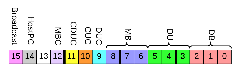
Fig. 23 Source/Destination address (16-bits)
Starting from least significant bit (LSB):
(2:0)   Detector Board Address
(5:3)   Detector Unit Address
(8:6)   Multiplexer Board Address
(9)     Detector Unit Controller source/destination flag
(10)    Coincidence Unit Controller source/destination flag
(11)    Coincidence Detector Unit Controller source/destination flag
(12)    Multiplexer Board Controller source/destination flag
(13)    Not used
(14)    Host PC source/destination flag
(15)    Broadcast flag
If the Broadcast flag is set in the destination address, the source node will pass the command down to all of its “children” and the child specified in the destination address will be read back to in order to create the response.
If the CUC or CDUC flags are set in the destination address, that corresponding unit will execute the command and respond. Namely, the response will not come from the unit specified in the destination address.
Finally, the payload is a 32-bit number that specifies additional information for each command; see below for examples.
Any operating system (Windows, GNU/Linux, or Mac OS) and programmable language (C, C++, Delphi, MATLAB, VB.NET, VC#, and Delphi) supported by QuickUSB can be used to interface with the OpenPET system. OpenPET provides multiple methods to control and configure the system. The simplest method is to use openpet.exe which is a Microsoft Windows executable that can configure and acquire data from an OpenPET system. Additionally, platform independent example Python scripts are also provided to streamline the configuration and acquisition process.
The executable openpet is used to control and configure the system. It has several optional arguments, list them by running openpet with -h or --help switches:
usage: openpet.py [-h] [-v] [-L] [-l] [-d DEVICEINDEX | -i INTERFACEINDEX]
    [-D IP]
    [-c ID DST PAYLOAD | -a DURATION | -sr FILE DST SIZE OFFSET | -sw FILE DST OFFSET]
    [-o FILE] [-t TIMEOUT] [-n RETRIES]

optional arguments:
  -h, --help            show this help message and exit
  -v, --verbose         Show debugging info.
  -L, --List            List network devices.
  -l, --list            List quickusb devices.
  -d DEVICEINDEX, --device DEVICEINDEX
                                                Quickusb device index.
                                                List devices to see indexes.
                                                DEFAULT=0
  -i INTERFACEINDEX, --interface INTERFACEINDEX
                                                Network interface device index.
                                                List devices to see indexes.
  -D IP, --destination IP
                                                IPv4 address of of destination node.
  -c ID DST PAYLOAD, --command ID DST PAYLOAD
                                                Sends a command to a destination
                                                module with a specific payload.
  -a DURATION, --acquire DURATION
                                                Acquire data for the specified
                                                duration (in seconds). Partial
                                                seconds are OK.
  -sr FILE DST SIZE OFFSET, --sram-read FILE DST SIZE OFFSET
                                                Reads SRAM contents from OpenPET and
                                                writes it to FILE.
  -sw FILE DST OFFSET, --sram-write FILE DST OFFSET
                                                Writes FILE contents to SRAM.
  -o FILE, --outputfile FILE
                                                File name to save acquired data.
  -t TIMEOUT, --timeout TIMEOUT
                                                Timeout duration (in seconds) between
                                                retries. Partial seconds are OK.
                                                DEFAULT=0.200
  -n RETRIES, --retries RETRIES
                                                Number of times I should try to
                                                contact OpenPET System before
                                                giving up. DEFAULT=20
Tables 8.1 and 8.2 show a list of the current OpenPET commands, including their command ID and a brief description of their function. The payload is specified for each command in the examples that follow.
| IDs | Name | Function |
|---|---|---|
| 0x0001 | Ping | Sends a single ping request to destination.
|
| 0x0002 | Write Children Bitstream | Command Support Board(s) to configure
all children boards from bitstream
stored in EPCS.
|
| 0x0003 | Write System Acquisition Mode | Sets the system mode register in
firmware to idle, scope, singles, etc.
|
| 0x0004 | Read System Acquisition Mode | Gets the system mode register
from firmware.
|
| 0x0005 | Write System Acquisition Mode Settings | Sets the system mode settings
register in firmware for the
mode selected.
|
| 0x0006 | Read System Acquisition Mode Settings | Gets the system mode settings
register from firmware.
|
| 0x0007 | Write System Acquisition Mode Action | Sets the system mode action register in
firmware to reset, start, stop.
|
| 0x0008 | Read System Acquisition Mode Action | Gets the system mode action register
from firmware.
|
| 0x0009 | Write Trigger Mask | Sets a mask to suppress triggers.
|
| 0x000A | Read Trigger Mask | Gets the mask from firmware.
|
| 0x000B | Write SRAM Data | Writes to external SRAM device.
Auto-increments address.
|
| 0x000C | Read SRAM Data | Reads from external SRAM device.
Auto-increments address.
|
| 0x000D | Zero out SRAM | SRAM content is zeroed out.
|
| 0x000F | Reset | Reset all configurations.
|
| 0x0101 | Write TDC Configuration | Sets the TDC control register.
|
| 0x0102 | Read TDC Configuration | Gets the TDC control register.
|
| 0x0103 | Reset ADC Configuration | Command Detector Boards(s) to set ADCs
registers to OpenPET default values.
|
| 0x0104 | Write ADC Register | Writes a register directly on ADC(s).
See ADC datasheet for
valid register maps.
|
| 0x0105 | Reset DAC Configuration | Command Detector Board(s) to set DACs
registers to OpenPET default values.
|
| 0x0106 | Write DAC Register | Write a register directly on DAC(s).
See DAC datasheet for
valid register maps.
|
| 0x0107 | Write Sawtooth pulse(s) | Command DAC(s) to send sawtooth
pulses for a given duration of time.
|
| 0x0108 | Write Firmware Threshold | Sets a firmware threshold level
to trigger on.
|
| 0x0109 | Read Firmware Threshold | Gets the firmware trigger threshold.
|
| IDs | Name | Function |
|---|---|---|
| 0x0000 | (Reserved) Busy | Child doesn’t have anything to reply yet.
|
| 0xFFFF | (Reserved) Dead | Dead, nonexistent, or not programmed.
|
| 0x7F00 | SW Command is Unknown | Software (Running on NIOS) command id
is unknown to node.
|
| 0x7F01 | SW Command Timed Out | Software (Running on NIOS) command id
has timed out.
|
| 0x7F02 | Targeted Child is Dead | Targeted child is dead, nonexistent,
or not programmed.
|
| 0x7F03 | Targeted Child is Busy | Targeted child is busy processing
previous command.
|
| 0x7F04 | FW Command is Unknown | Firmware (Running on FPGA fabric)
command id is unknown to node.
|
| 0x7F05 | FW Command Timed Out | Firmware (Running on FPGA fabric)
command id has timed out.
|
| 0x7F06 | SW incomplete packet | Software (Running on NIOS) received
incomplete OpenPET command
|
| 0x7F07 | SW interrupt
routine can’t keep up
|
Software (Running on NIOS) received packets
faster than it can handle.
|
Description and Examples of Command IDs
Command ID: 0x0001
Description: Sends a single ping request to destination. If broadcast on DST was specified, then the read back will be performed on the address provided.
Payload: None e.g. 0 or any value.
Examples:
Send a ping command using the openpet executable to destination 0x0002 i.e., DB in slot 2 with 0 payload. openpet will print out the date, time, message type, [S]ENT or [R]ECEIVED indicator, command id, destination (when sending) or source (when receiving) address, and the payload. Note that the MSB of the command ID is set to ‘1’ when receiving.:
$ openpet -c 0x0001 0x0002 0

2015-09-01 12:30:00,529 INFO [S] 0x0001 0x0002 0x00000000
2015-09-01 12:30:00,733 INFO [R] 0x8001 0x0002 0x00000000
Just like the first example, however, using decimal numbers instead of hex:
$ openpet -c 1 2 0
The destination address has the broadcast flag set to 1. This will cause the SB to send the ping command to all its children, however, the reply will be read back only from 0x0002:
$ openpet -c 0x0001 0x8002 0
The asynchronous flag in the command id is set to 1. This will cause the SB to immediately respond to the HostPC regardless if the ping command was successful on 0x0002 or not. This feature becomes useful when sending commands that take minutes to complete. Note, that the targeted destination will not be able to respond until it completes the execution of the asynchronous command, however, other nodes can be accessed and controlled independently:
$ openpet -c 0x1001 0x0002 0
QuickUSB device index 1 is used instead of the default device:
$ openpet -d 1 -c 1 2 0
Using Ethernet instead of default QuickUSB device. By default the IP address of the OpenPET chassis is 10.10.10.2:
$ openpet -D 10.10.10.2 -c 1 2 0
The HostPC is willing to wait 1 second for the SB to provide a valid reply. The default timeout per try is 200ms:
$ openpet -t 1 -c 1 2 0
The HostPC tries a maximum of 3 times before giving up on the SB. The wait between each trial is 0.5 second:
$ openpet -n 3 -t 0.5 -c 1 2 0
More debugging information is displayed:
$ openpet -v -c 1 2 0
Command ID: 0x0002
Description: FPGA bitstream configuration is read from EPCS flash memory then written to all children. This command is executed on power-up by default.
Payload: None e.g. 0 or any value.
Examples:
Ask CDUC to configure all of its children i.e., detectorboard FPGAs (not io):
$ openpet -c 2 0x0800 0
Command ID: 0x0003
Description: Writes the System Acquisition Mode register in firmware.
Payload:

Fig. 24 System Acquisition Mode payload
Starting from least significant bit (LSB)
(3:0)  Mode
(31:4) not used
Available Modes:
IDLE 0x0 Oscilloscope 0x1 Singles 0x2
Examples:
Broadcast to all nodes to set System Acquisition Mode to scope mode. The command acknowledgment is received from DB in slot 3:
$ openpet -c 3 0x8003 1
Command ID: 0x0004
Description: Reads the System Acquisition Mode register from firmware.
Payload: None e.g. 0 or any value.
Examples:
Read the System Acquisition Mode register from firmware from slot 5. The payload of the reply is the mode that was previously set i.e., 1=scope mode:
$ openpet -c 4 5 0xDEADFEED

2015-09-02 11:10:00,528 INFO [S] 0x0004 0x0005 0xDEADFEED
2015-09-02 11:10:00,732 INFO [R] 0x8004 0x0005 0x00000001
Command ID: 0x0005
Description: Writes the System Acquisition Mode Settings register in firmware. The 32-bit setting payload value depends on the mode set in Command ID 0x0003.
Payload:
- Payload when System Acquisition Mode = 0x1 = Oscilloscope (scope mode):

Fig. 25 System Acquisition Mode Settings payload for oscilloscope mode
Starting from least significant bit (LSB)
(3:0)   Reserved: Must be 0001
(12:4)  Total Number of ADC samples, see notes below (zero is accounted for)
(15:13) Reserved
(19:16) Number of ADC samples before energy trigger (2^4 = 16)
(23:20) Reserved
(27:24) Trigger window (2^4 = 16)
(31:28) Reserved
- Payload when System Acquisition Mode = 0x2 = Singles (singles mode):

Fig. 26 System Acquisition Mode Settings payload for singles mode
Starting from least significant bit (LSB)
(3:0)   Total number of ADC clock ticks to finish a single Event computation
        (2^4 = 16)
(7:4)   Reserved, max ADC clock ticks to process data (2^8 = 256)
(15:8)  Reserved
(31:16) Not Used
Note
- Scope Mode:
- Total Number of samples should be greater than samples before trigger + trigger window.
- Total Number of samples should not exceed Firmware’s maximum number of samples - (Number of Channel headers + Detector Board Header)
- Singles Mode:
- Event computation clocks ticks should be greater than 1.
- Number of pipeline stages is pre-defined in the firmware as a constant
- PipelineStages = ceil(EventCompuationClockTicks/SliceWidth) + 1 , where ceil() rounds the number to the next highest integer.
Examples:
Broadcast to all nodes to set System Acquisition Mode to scope mode. Then use data format = 1, 16 samples, 0 samples before trigger, and a trigger window to 2:
$ openpet -c 3 0x8003 1
$ openpet -c 5 0x8003 0x02000101
Broadcast to all nodes to set System Acquisition Mode to singles mode. Then TODO FIXME:
$ openpet -c 3 0x8003 2
$ openpet -c 5 0x8003 0x00000001
Note
If the user sets a parameter with a value that is too large, the system will set the parameter to the maximum possible value. This will be evident in the response payload. It will show the maximum possible value instead of the user’s value. The user can then decide to continue or change it.
Command ID: 0x0006
Description: Reads the System Acquisition Mode Settings register from firmware.
Payload: None e.g. 0 or any value.
Examples:
Reads the System Acquisition Mode Settings register from firmware from slot 3. The payload of the reply is set to the settings previously specified, e.g., scope mode settings:
$ openpet -c 6 3 0xDEADFEED

2015-09-02 11:10:00,528 INFO [S] 0x0006 0x0003 0xDEADFEED
2015-09-02 11:10:00,732 INFO [R] 0x8006 0x0003 0x02000101
Command ID: 0x0007
Description: Writes the System Acquisition Mode Action register in firmware.
Payload:

Fig. 27 System Acquisition Mode Action payload
Starting from the least significant bit (LSB)
(3:0)  Action
(31:4) not used
Available actions:
Reset 0x0 Stop 0x1 Run 0x2
Examples:
Reset the System Acquisition Mode and Settings (payload = 0x0):
$ openpet -c 7 0x8003 0x00000000
Stop the current system acquisition (payload = 0x1):
$ openpet -c 7 0x8003 0x00000001
First, broadcast to all nodes to set System Acquisition Mode to scope mode. Then use data format = 0, 16 samples, 0 samples before trigger, and a trigger window to 2. Finally, run the acquire data command (payload = 0x2):
$ openpet -c 3 0x8003 1
$ openpet -c 5 0x8003 0x02000100
$ openpet -c 7 0x8003 0x00000002
Command ID: 0x0008
Description: Reads the System Acquisition Mode Action register from firmware.
Payload: None e.g. 0 or any value.
Examples:
Reads the System Acquisition Mode Action register from firmware from slot 3. The payload of the reply is set to the action previously specified, e.g., reset = 0:
$ openpet -c 8 3 0xDEADFEED

2015-09-02 11:10:00,528 INFO [S] 0x0008 0x0003 0xDEADFEED
2015-09-02 11:10:00,732 INFO [R] 0x8008 0x0003 0x00000000
If action previously set to terminate the current action, e.g., stop = 1:
$ openpet -c 8 3 0xDEADFEED

2015-09-02 11:10:00,528 INFO [S] 0x0008 0x0003 0xDEADFEED
2015-09-02 11:10:00,732 INFO [R] 0x8008 0x0003 0x00000001
If action previously set to run the system acquisition, e.g., run = 2:
$ openpet -c 8 3 0xDEADFEED

2015-09-02 11:10:00,528 INFO [S] 0x0008 0x0003 0xDEADFEED
2015-09-02 11:10:00,732 INFO [R] 0x8008 0x0003 0x00000002
Command ID: 0x0009
Description: Writes a mask to suppress triggers in firmware.
Payload:

Fig. 28 Trigger mask payload
Starting from the least significant bit (LSB)
(31:0) 1 bit per channel.  Set bit to 1 to enable trigger on that channel.
Example:
Set trigger masks for channels 0, 5, and 8 in detector board 5:
$ openpet -c 9 5 0x00000121
Command ID: 0x000A
Description: Reads the trigger mask from firmware.
Payload: None e.g. 0 or any value.
Example:
Reads the trigger mask previously set in detector board 5:
$ openpet -c 10 5 0xDEADFEED

2015-09-02 11:10:00,528 INFO [S] 0x000A 0x0005 0xDEADFEED
2015-09-02 11:10:00,732 INFO [R] 0x800A 0x0005 0x00000121
Command ID: 0x000B
Description: Writes to external SRAM device. Auto-increments address.
Payload:
Starting from the least significant bit (LSB)
(31:0) Value to write to SRAM
Caveats: The Mode Action has to be in Reset for this command to work correctly.
Example:
Write some value to external SRAM in detector board 1:
$ openpet -c 11 1 0x12345678

2015-10-12 11:02:33,115 INFO [S] 0x000B 0x0001 0x12345678
2015-10-12 11:02:33,355 INFO [R] 0x800B 0x0001 0x12345678
- Alternative: -sw option
Write to SRAM in detector board 1 from file sramtest.bin starting from the top (offset = 0):
$ openpet -sw sramtest.bin 1 0

2015-10-12 11:05:22,956 INFO Writing content to SRAM.
2015-10-12 11:05:28,385 INFO Done SRAM writing.
Command ID: 0x000C
Description: Reads from external SRAM device. Auto-increments address.
Payload:
Starting from the least significant bit (LSB)
(31:0) SRAM address
Caveats: The Mode Action has to be in Reset for this command to work correctly.
Example:
Read data starting from SRAM address 0 in detector board 1:
$ openpet -c 12 1 0

2015-10-12 11:02:41,956 INFO [S] 0x000C 0x0001 0x00000000
2015-10-12 11:02:42,165 INFO [R] 0x800C 0x0001 0x12345678
- Alternative: -sr option
Read 100 values from SRAM to file sramtest.bin from detector board 1 starting from the top (offset = 0):
$ openpet -sr sramtest.bin 1 100 0

2015-10-12 11:03:11,296 INFO Reading SRAM content.
2015-10-12 11:03:15,635 INFO Done Reading SRAM Content.
Command ID: 0x000D
Description: Clears SRAM content. Sets to zero.
Payload: None e.g. 0 or any value.
Example:
Clears SRAM content on detector board 1:
$ openpet -c 13 1 0xDEADFEED

2015-10-09 11:10:00,528 INFO [S] 0x000D 0x0001 0xDEADFEED
2015-10-09 11:10:00,732 INFO [R] 0x800D 0x0001 0x00000000
Command ID: 0x000F
Description: System wide reset. It resets the configurations of firmware, software, and peripheral hardware to default values:
**Payload**: None e.g. 0 or any value.
Example:
Broadcast a reset to all nodes and get a reply from 0x1:
$ openpet -c 0xF 0x8001 0

2015-10-09 11:10:00,511 INFO [S] 0x000F 0x8001 0x00000000
2015-10-09 11:10:00,733 INFO [R] 0x800F 0x8001 0x00000000
Command ID: 0x0101
Description: Sets the TDC control register.
Payload:

Fig. 29 Payload for TDC control register
Starting from the least significant bit (LSB)
(7:0)   TDC command
(31:8)  Not used
Available TDC commands:
Reset 0x80 Calibrate 0x02 Run 0x04
Examples:
Set the TDC control register to reset in detector board 5:
$ openpet -c 0x0101 5 0x00000080
Set the TDC control register to calibrate in detector board 5:
$ openpet -c 0x0101 5 2
Set the TDC control register to run in detector board 5:
$ openpet -c 0x0101 5 4
Command ID: 0x0102
Description: Gets the TDC control register.
Payload: None e.g. 0 or any value.
Example:
Reads the current TDC control register from detector board 5, e.g., run = 1:
$ openpet -c 0x0102 5 0xDEADFEED

2015-10-09 11:10:00,528 INFO [S] 0x0102 0x0005 0xDEADFEED
2015-10-09 11:10:00,732 INFO [R] 0x8102 0x0005 0x00000001
Command ID: 0x0103
Description: Resets ADC configuration. Commands Detector Board(s) to set ADC registers to OpenPET default values.
Payload: None e.g. 0 or any value.
Example:
Resets ADC registers on detector board 3 to default OpenPET values:
$ openpet -c 0x0103 3 0xDEADFEED

2015-10-09 11:10:00,528 INFO [S] 0x0103 0x0003 0xDEADFEED
2015-10-09 11:10:00,732 INFO [R] 0x8103 0x0003 0x00000000
Command ID: 0x0104
Description: Writes ADC register. See ADS5282 datasheet for valid register maps.
Payload:

Fig. 30 Payload to write ADC register
Starting from the least significant bit (LSB)
(15:0)   ADC data (see ADS5282 datasheet, page 17)
(17:16)  Reserved
(25:18)  ADC register address (see ADS5282 datasheet, page 17)
(26)     Reserved
(27)     ADC chip address (0 for channel 0-7; 1 for channel 8-15)
(29:28)  Reserved
(30)     Not used
(31)     Broadcast flag, i.e., run on all ADC chips
Note
The ADC address and ADC data for the corresponding DB channel when setting the ADC gain. Each gain is set using 4 bits ranging from 0-12 dB. The gain has to be set on four channels at a time (i.e., 16-bit ADC data).
| ADC Chip Address | ADC Address | ADC Data (MSB to LSB) |
|---|---|---|
| 0x0 | 0x2A | Channel 3 to 0 |
| 0x0 | 0x2B | Channel 4 to 7 |
| 0x1 | 0x2A | Channel 11 to 8 |
| 0x1 | 0x2B | Channel 12 to 15 |
Examples:
Sets the ADC gain to 6 dB for channels 4 to 7 on the Detector Board in slot 3 without broadcasting:
$ openpet -c 0x0104 0x0003 0x00AC6666
- Payload breakdown (LSB to MSB):
- 0x00AC6666 (=0 0 00 0 0 00101011 00 0110011001100110)
- Bits 15-0: 0110011001100110 (see ADS5282 datasheet, page 17)
- Bits 17-16: Reserved
- Bits 25-18: 0x2B indicates for channel 4 to 7
- Bits 26: Reserved
- Bits 27: 0 indicates for channel 4 to 7
- Bits 29-28: Reserved
- Bits 30: Not used
- Bits 31: 0 indicates not a broadcast command
Sets the ADC gain to 8 dB for channels 8 to 11 on the Detector Board in slot 5 with broadcasting:
$ openpet -c 0x0104 0x0005 0x88A88888
- Payload breakdown (LSB to MSB):
- 0x88A88888 (=1 0 00 1 0 00101010 00 1000100010001000)
- Bits 15-0: 1000100010001000 (see ADS5282 datasheet, page 17)
- Bits 17-16: Reserved
- Bits 25-18: 0x2A indicates for channel 8 to 11
- Bits 26: Reserved
- Bits 27: 1 indicates for channel 8 to 11
- Bits 29-28: Reserved
- Bits 30: Not used
- Bits 31: 1 indicates broadcast command
Command ID: 0x0105
Description: Resets DAC configuration. Commands Detector Board(s) to set DAC registers to OpenPET default values.
Payload: None e.g. 0 or any value.
Example:
Resets DAC registers on detector board 3 to default OpenPET values:
$ openpet -c 0x0105 3 0xDEADFEED

2015-10-09 11:10:00,528 INFO [S] 0x0105 0x0003 0xDEADFEED
2015-10-09 11:10:00,732 INFO [R] 0x8105 0x0003 0x00000000
Command ID: 0x0106
Description: Writes DAC register. See DAC LTC2634 datasheet for valid register maps.
Payload:

Fig. 31 Payload to write DAC register
Starting from the least significant bit (LSB)
(9:0)   DAC data (see LTC2634 datasheet, page 20)
(12:10) Reserved
(16:13) DAC address (see LTC2634 datasheet, page 20)
(20:17) DAC command (see LTC2634 datasheet, page 20)
(22:21) Reserved
(26:23) DAC chip address
(28:27) DAC type (00=energy, 01=timing, 10=reserved, 11=all)
(30:29) Not used
(31)    Broadcast flag, i.e., run on all DAC chips for a given type
Note
DAC Command=0x3 to set DAC voltage (10-bit data)
| Type | Bits 28-27 | DAC Full Scale |
|---|---|---|
| Energy | 00 | 4.096 V |
| Timing | 01 | 2.500 V |
| Reserved | 10 | 2.500 V |
The DAC address and DAC chip select for the corresponding DB channel when setting the energy and timing DAC. Because a chip has four DAC, a single DAC voltage can be set to four channels with one command.
| Channel | DAC Address | DAC Chip Address |
|---|---|---|
| 0 | 0x0 | 0x0 |
| 1 | 0x1 | 0x0 |
| 2 | 0x2 | 0x0 |
| 3 | 0x3 | 0x0 |
| 4 | 0x0 | 0x1 |
| 5 | 0x1 | 0x1 |
| 6 | 0x2 | 0x1 |
| 7 | 0x3 | 0x1 |
| 8 | 0x0 | 0x2 |
| 9 | 0x1 | 0x2 |
| 10 | 0x2 | 0x2 |
| 11 | 0x3 | 0x2 |
| 12 | 0x0 | 0x3 |
| 13 | 0x1 | 0x3 |
| 14 | 0x2 | 0x3 |
| 15 | 0x3 | 0x3 |
| 0-3 | 0xF | 0x0 |
| 4-7 | 0xF | 0x1 |
| 8-11 | 0xF | 0x2 |
| 12-15 | 0xF | 0x3 |
- The timing DAC is usually set to a low threshold to obtain the best timing.
- The energy DAC determines whether readout is initiated, and so is usually set to a higher threshold to reduce noise triggers (see 16-Channel Detector Board).
Examples:
Sets DAC energy threshold to +1.150V for channel 4 on the Detector Board in slot 3 without broadcasting:
$ openpet -c 0x0106 0x0003 0x00860120
- Payload breakdown (LSB to MSB):
- 0x000860120 (=0 00 00 0001 00 0011 0000 000 0100100000)
- Bits 9-0: 0100100000 (1024*1.15/4.096)
- Bits 12-10: Reserved
- Bits 16-13: 0x0 (channel 4 in chip select 0x1)
- Bits 20-17: 0x3 (see DAC LTC2634 datasheet, page 20)
- Bits 22-21: Reserved
- Bits 26-23: 0x1 indicates this is the chip where channel 4 resides
- Bits 28-27: 00 indicates that the DAC type is energy
- Bits 30-29: Not used
- Bits 31: 0 indicates not a broadcast command
Sets DAC timing threshold to +0.5V for channel 12 on the Detector Board in slot 5 with broadcasting:
$ openpet -c 0x0106 0x0005 0x898600CD
- Payload breakdown (LSB to MSB):
- 0x898600CD (=1 00 01 0011 00 0011 0000 000 0011001101)
- Bits 9-0: 0011001101 (1024*0.5/2.5)
- Bits 12-10: Reserved
- Bits 16-13: 0x0 (channel 12 in chip select 0x3)
- Bits 20-17: 0x3 (see DAC LTC2634 datasheet, page 20)
- Bits 22-21: Reserved
- Bits 26-23: 0x3 indicates this is the chip where channel 12 resides
- Bits 28-27: 01 indicates that the DAC type is timing
- Bits 30-29: Not used
- Bits 31: 1 indicates a broadcast command
Command ID: 0x0107
Description: Writes Sawtooth pulse(s). Commands DAC(s) to send sawtooth pulse(s) for a given duration of time.
Payload:

Fig. 32 Payload to write sawtooth pulse
Starting from the least significant bit (LSB)
(3:0)   DAC chip address
(5:4)   DAC type
(13:6)  Number of sawtooth pulses to send
(30:14) Not used
(31)    Broadcast flag, i.e., run on all DAC chips for a given type
Note
The time it takes to execute and finish this command depends on the number of sawtooth pulses you request. It is highly advised to send this command as an asynchronous command (non-blocking) by setting the MSB on CMD ID to ‘1’.
Example:
Command DAC to send 100 sawtooth pulses to detector board 3. DAC type is 00 which is energy, and chip address is 0x2. Broadcast flag is set to 1, and the CMD ID MSB is set to 1 for asynchronous command:
$ openpet -c 0x8107 0x0003 0x80001902
Command ID: 0x0108
Description: Sets a firmware threshold level to trigger on.
Payload:

Fig. 33 Payload to set firmware trigger threshold
Starting from the least significant bit (LSB)
(11:0)   Threshold value
(15:12)  Reserved
(17:16)  Mode (00=off, 01=on)
(31:18)  Not used
Note
The minimum and maximum threshold values correspond to the minimum and maximum of the ADC signal which is 2Vpp. The 0V value is in the middle so to set at the 0V DC, set the MSB of the threshold value to 1. To set the maximum threshold value (1V), flip all bits 0 to 11 to 1. To set the minimum threshold value (-1V), flip all bits 0 to 11 to 0.
Example:
Sets the firmware threshold level to 0V and mode ‘on’ for detector board 5:
$ openpet -c 0x0108 0x0005 0x00010800
Command ID: 0x0109
Description: Gets the firmware trigger threshold.
Payload: None e.g. 0 or any value.
Example:
Retrieves the firmware trigger threshold previously set on detector board 5:
$ openpet -c 0x0109 0x0005 0xDEADFEED

2015-10-09 11:10:00,528 INFO [S] 0x0109 0x0005 0xDEADFEED
2015-10-09 11:10:00,732 INFO [R] 0x8109 0x0005 0x00010800
Data Modes
There are different data-gathering modes that can be created and used with the OpenPET system. Currently, there are three modes available with 232 modes possible.
Mode Type Data Description Scope Mode Raw ADC data Singles Mode Processed ADC data, e.g., energy Idle Mode Nothing processed or transferred
For each mode, there are actions that can be performed. Again, there are 232 actions possible with three available so far.
Action Description Run Launches a selected Mode Stop Causes a selected Mode to pause Reset Causes a selected Mode to reset to default
The settings for a selected mode is stipulated by a 32-bit word that is described in each mode section
Scope Mode
In Scope mode, raw ADC data is sent to an external disk. The data file is a binary file and shown in Fig. 34. It is a simple 32-bit format for easy parsing and manipulation. The headers are prepended to the raw data including information such as time of acquisition and all the acquisition settings. There is 4KB reserved for user defined content.
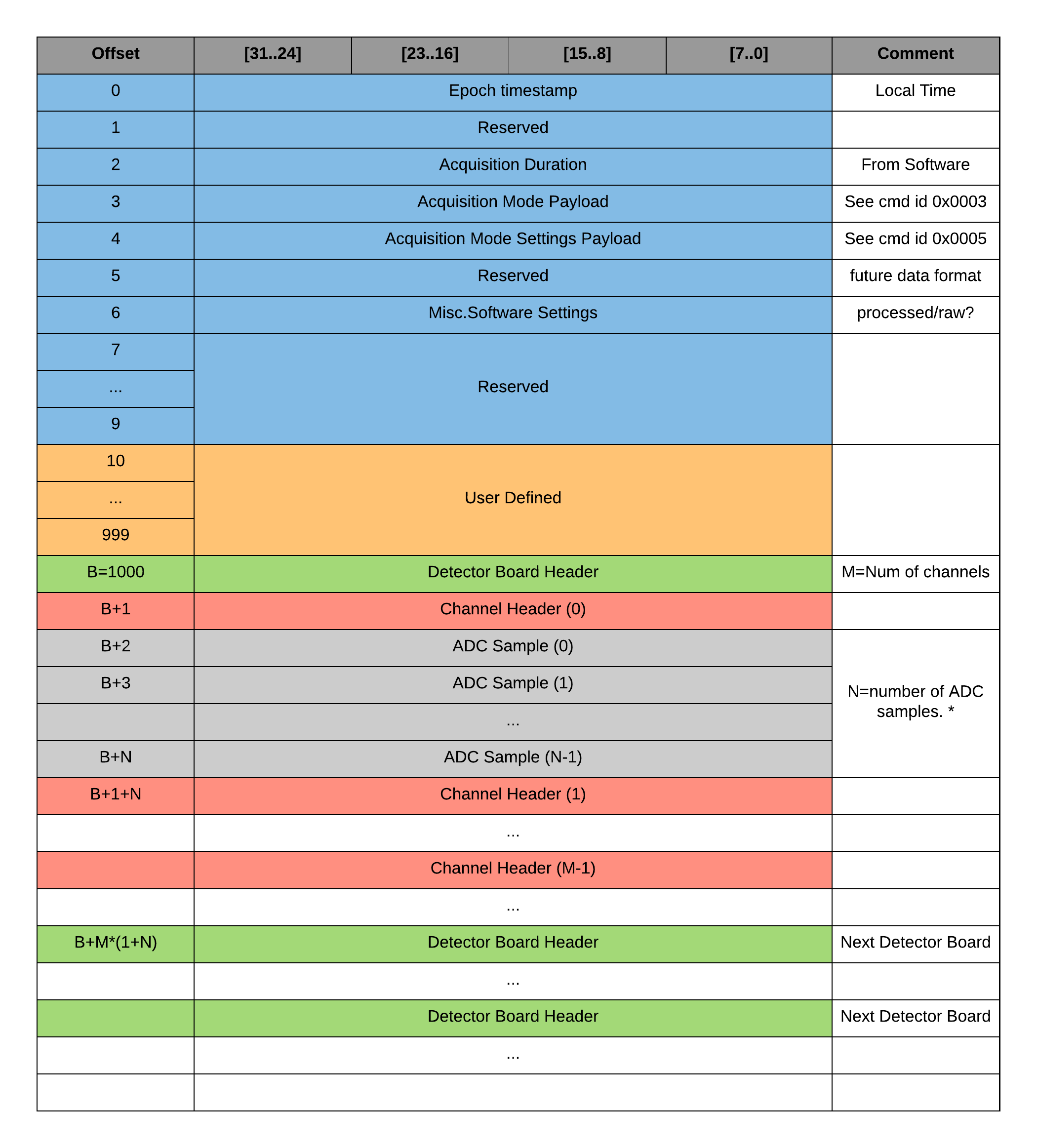
Fig. 34 Binary file format for scope mode
It uses a 16-bit wide bus to transfer 32-bits at a time via DDR. Each 32-bit packet has a 4-bit packet ID. Each detector board wraps its data with a DB header, and each channel in a given detector board wraps its data with a channel header (Fig. 35). All detector boards are synchronized when they start the acquisition.
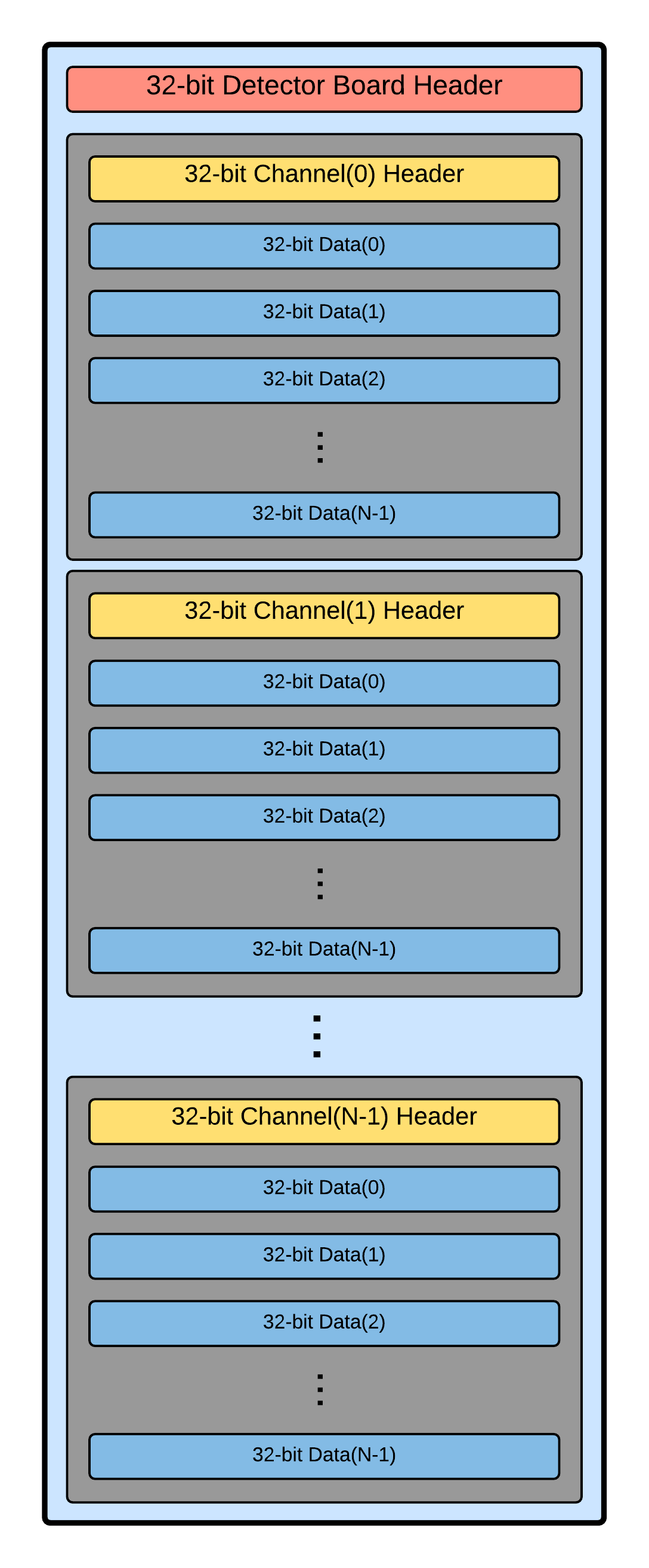
Fig. 35 Visual representation of the raw data from one detector board.
Fig. 36, Fig. 37, and Fig. 38 show the bit maps of the headers and data pack mentioned above.
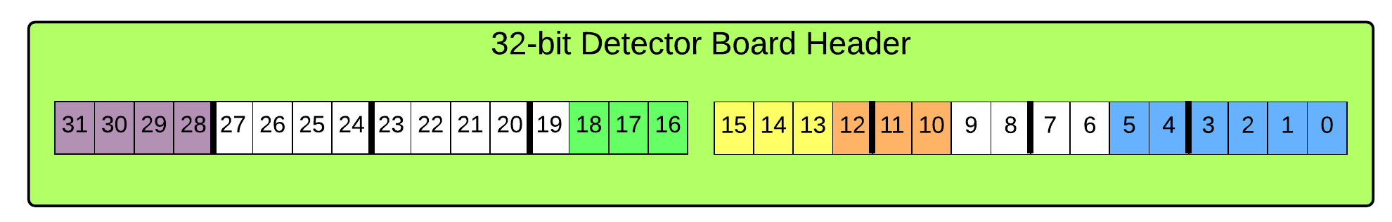
Fig. 36 Detector board header in scope mode
Starting from the least significant bit (LSB)
(5:0)   Number of channel header packets (i.e., 0 to 63)
(9:6)   Not used
(12:10) Detector board address (populated by parent)
(15:13) DU address (populated by parent)
(18:16) MB address (populated by parent)
(27:19) Not used
(31:28) Packet ID (must equal 0x4)
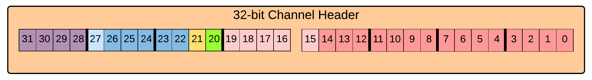
Fig. 37 Channel header in scope mode
Starting from the least significant bit (LSB)
(19:0)  TDC data (currently using (14:0) with (19:15) for expansion)
(20)    Hardware trigger hit (energy)
(21)    Firmware trigger hit
(27:22) Channel address (i.e., 0 to 63)
(31:28) Packet ID (must equal 0x3)
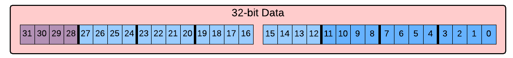
Fig. 38 Data packet in scope mode. In this example, the raw ADC data is from (11:0)
Starting from the least significant bit (LSB)
(27:0)  Raw ADC data
(31:28) Packet ID (must equal 0x1)
For a given 32-bit packet or header, the Packet ID is the four most significant bits as shown in Fig. 39. It is used to verify the type of packet received at a parent. It also allows a node to identify, validate, and semi-confirm the integrity of the packet in the data path.
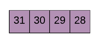
Fig. 39 Packet ID for scope mode. It is bits (31:28) for the scope headers and data packet above.
| ID | Description |
|---|---|
| 0x0 | Reserved. Do NOT use |
| 0x1 | ADC data |
| 0x2 | Reserved |
| 0x3 | Channel header |
| 0x4 | Detector board header |
| 0x5 | DUC header |
| 0x6 | CUC header |
| 0x7 | CDUC header |
| 0x8 | MBC header |
| 0x9 | Host PC header |
| 0xA-F | Not used |
The bit assignment for the scope mode settings are described below with Fig. 40. They are set using Command ID: 0x0005.

Fig. 40 Scope mode settings
Starting from the least significant bit (LSB)
(3:0)   Reserved (must equal 0001)
(12:4)  Total number of ADC samples (2^9 = 512; zero is accounted for)
(15:13) Reserved
(19:16) Number of ADC samples before energy trigger (2^4 = 16)
(23:20) Reserved
(27:24) Trigger window (2^4 = 16)
(31:28) Reserved
Note
- The total number of samples should be greater than the sum of the samples before the trigger and the trigger window.
- The total number of samples should not exceed the firmware’s maximum number of samples minus the sum of the channel and detector board headers.
Also, the FIFO stores the ADC samples along with the detector board and channel headers. Since the FIFO always has a fixed size dependent on the firmware, the number of ADC samples is limited. Therefore, if the FIFO maximum size is 32, and the user sets the total number of ADC samples to be 32, there will only be 15 ADC samples because 16 slots are taken up by the 16 channel headers, and 1 slot is filled with the detector board header. If the user sets to collect only 5 ADC samples, then there will be 5 samples since the FIFO has room for all five. The maximum number of ADC samples that can be acquired is actually the FIFO size minus 17 (16 channel headers and 1 detector board header).
In scope mode, the data is transferred through multiplexing that can be explained through a small system example. With a single chassis, the multiplexing occurs in the support board. There is no data loss. For the IO FPGAs, there are four inputs, one for each detector board, and one output going to the Main FPGA. For the Main FPGA, there are two inputs, one for each IO FPGA, and one output going to the Host PC. A basic schematic is shown in Fig. 41. The code is reusable on both the Main and IO FPGAs.
Two options are available for multiplexing. The default setting is a synchronized data management across all detector boards, i.e., an aligned readout on all detector boards. It is fair to random triggers (round-robin), biased toward periodic triggers, and has a longer dead time. The other option is a first-in-first-out scheduler. It is fair to periodic triggers, biased toward detector boards with higher trigger rates, and has a shorter dead time.
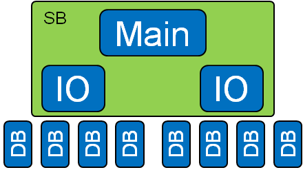
Fig. 41 Block diagram of a small system with the Main and IO FPGAs on the support board.
Data in the FPGAs is stored in a queue where the queue depth equals twice the number of inputs. For an IO FPGA, the queue depth is 8 (2*4 inputs), and for the Main FPGA, the queue depth is 4 (2*2 inputs). The code is generic and reusable for both FPGAs. As shown in Fig. 42, there is a write pointer and a read pointer. The write pointer tags an incoming block of data and then moves onto the next empty slot to tag the next incoming block of data. On the other end, once the data is read out, the queue slot is emptied and the read pointer advances to read the next block of data. These read and write pointers are circular pointers.

Fig. 42 Diagram of how data is read in the queue for scope mode.
Fig. 43 is the state machine diagram for the detector boards in scope mode.
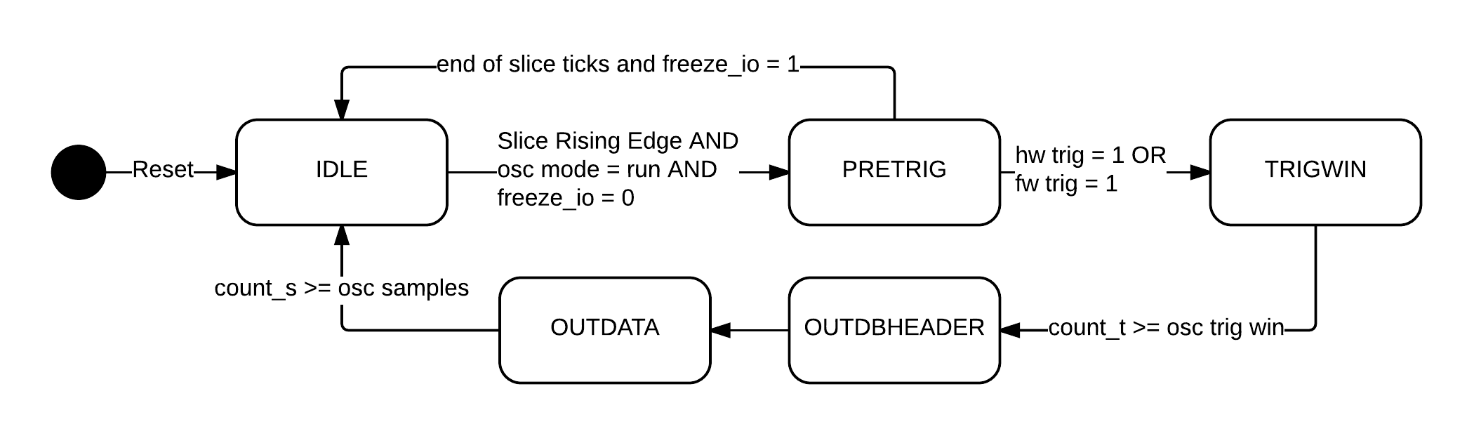
Fig. 43 Scope mode detector board state machine
It is initially in the IDLE stage where it is doing nothing but looking at the data coming into the system. It is not storing anything. There are three conditions that must be met for it to move onto the next stage. There must be a slice rising edge, the scope mode action must be set to RUN, and there cannot be a freeze input signal that restricts data flow. If these criteria are met, the next stage is the PRETRIG stage. Here, a user-defined number of samples before the trigger threshold are stored in the FIFO. The number of samples is set in the scope mode settings (Fig. 40) using bits (19:16). The FIFO can hold 256 samples, but in PRETRIG, it only stores the most recent 32 samples. Once a firmware or hardware trigger is detected on one channel, it moves on to the TRIGWIN stage. After that first trigger is detected, there is a set period of time (trigger window) where the system stores information from other channels that subsequently triggered. Again, this window is set in the scope mode settings using bits (27:24). Once this time window has lapsed, the information is outputted. The detector board header is read out first followed by the first channel header and all of its data. There is a counter (count_s) that increments until the number of ADC samples is reached so that it knows when all the data has been outputted. Once all the data has been read out, the next channel header is outputted with all of its data and so on until the final channel is read. After all the channels have been read, the detector board returns to the IDLE stage.
If there is no trigger in the PRETRIG stage and the freeze input is flipped to one, the detector board goes back to IDLE. The “freeze” command occurs when there is lack of memory space somewhere along the data flow. It can also occur when an external issue causes a disruption in data flow (e.g., unplugged cable).
The entire system freezes by default starting with the source of the error and flowing to the bottom of the hierarchy (parent to child). For example, looking at a small system (Fig. 41), if the Main FPGA runs out of memory, it will send a freeze command to both its IOs which in turn will freeze all of their detector boards. If something happens to the Host PC, it will send a freeze command down to the QuickUSB which sends it to the Main FPGA which will give it to all the IO FPGAs which freezes all the detector boards.
As mentioned earlier, if a freeze command is given, all detector boards are frozen by default. However, there is another option that freezes only select detector boards and lets the rest continue to send data.
Singles Mode
In Singles mode, processed ADC data is received from the system. There are two ‘slice’ widths supported, 128-bit words and 256-bit words. Like Scope mode, it sends 32 bits at a time using DDR where each 32-bit packet has a 4-bit packet ID. There are customizable pipeline stages depending on the processing needs (user or algorithm defined). User-defined cores are isolated from the Singles top level core.
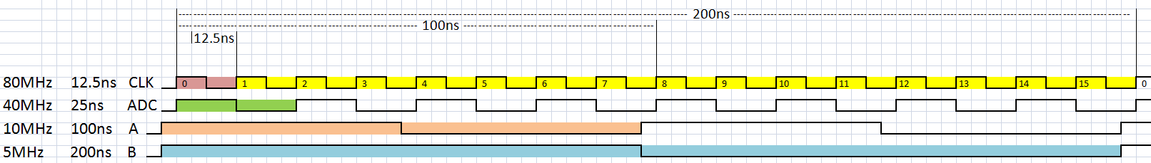
Fig. 44 Clock-Slice relationships. Slices A and B are 3.125ns early. In A, we can handle 4 ADC samples (12-bits each). In B, we can handle 8 ADC samples.
The data file is a binary file depicted in Fig. 45. It has similar characteristics to the scope mode data file. There are headers prepended to the singles data including time of acquisition and all acquisition settings. It is a simple 32-bit format for easy parsing and manipulation. Again, there is 4KB reserved for user-defined content.
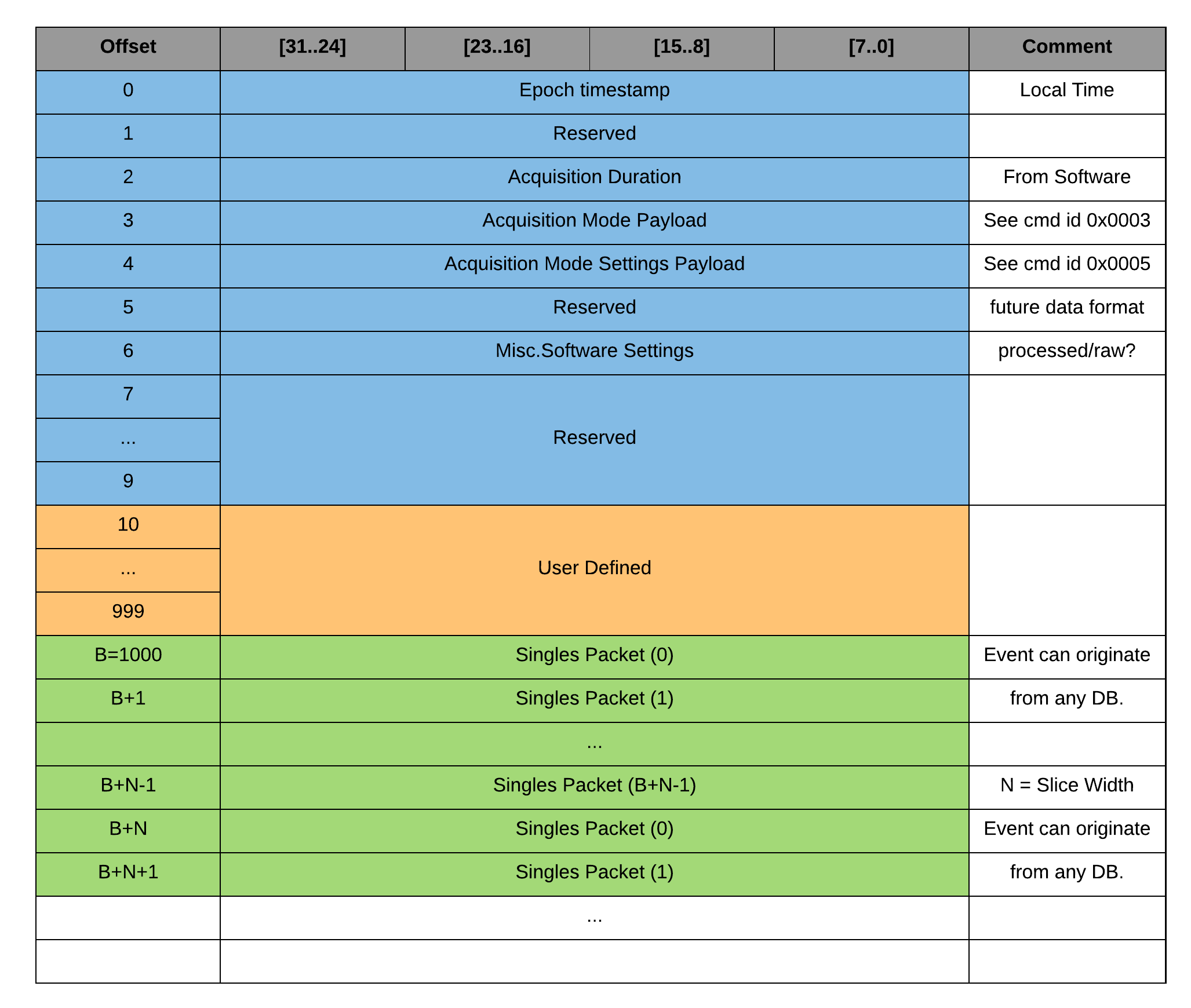
Fig. 45 Binary file format in singles mode
Each individual piece of data recorded or event is either a 128-bit or 256-bit word. This word is broken up into N number of 32-bit packets as show in Fig. 46. As mentioned above, each packet has a 4-bit packet ID.

Fig. 46 Diagram of a singles mode word. There are N number of 32-bit packets where N starts at 0.
Below is a table showing the differences between the two slice choices or word sizes. It also shows how to calculate the number of packets N and the total bits transferred per slice.
- R = System Clock Period/ADC Clock Period
- N = R * Slice Period/System Clock Period
| Characteristics | Slice Choice 1 | Slice Choice 2 |
|---|---|---|
| Default System Clock Period | 12.5ns (80MHz) | 12.5ns (80MHz) |
| Default ADC Clock Period | 25ns (40MHz) | 25ns (40MHz) |
| Slice Period | 100ns (10MHz) | 200ns (5MHz) |
| R | 12.5/25 = 1/2 | 12.5/25 = 1/2 |
| N (Number of Packets) | 1/2 * 100/12.5 = 4 packets | 1/2 * 200/12.5 = 8 packets |
| Total Bits Transferred per Slice | 4*32 = 128 bits | 8*32 = 256 bits |
As in scope mode, the Packet ID is used to verify the type of packet received at a parent. It also allows a node to identify, validate, and semi-confirm the integrity of the packet in the data path. The table below lists current IDs.
Fig. 47 Packet ID for singles mode. It is the four most significant bits in a 32-bit packet.
| ID | Description |
|---|---|
| 0x0 | Reserved. Do NOT use |
| 0x1 | Singles Packet |
| 0x2-F | Not used |
Data received in singles mode uses arbitration to store it. This arbitration can be examined through a small system example. For a single chassis, arbitration happens in the support board. For an IO FPGA, there are four inputs, one from each detector board, and one output to the Main FPGA. For the Main FPGA, there are two inputs, one from each IO FPGA, and one output to the Host PC (Fig. 41). In this method, there is loss of data. The code on the Main and IO FPGAs is reusable.
The arbitrator uses a true random number generator to select one incoming event. No priority is given to any input slot. It works for all cases (e.g., 1-in-1-out, 2-in-1-out, 3-in-1-out, 4-in-1-out). Only one clock cycle is required for selection.
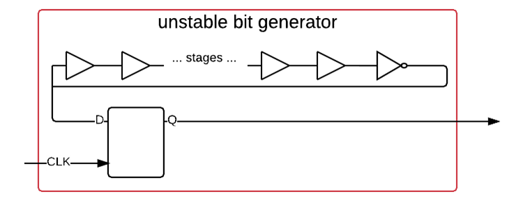
Fig. 48 Unstable bit generator used in the random selector
Fig. 48 is a diagram of the unstable bit generator used in the random selector (Fig. 49) for the arbitrator. It uses a programmable number of ring oscillator stages, and randomness is created from voltage, temperature, and near-by-logic variations. The output bit Q is unstable by design.
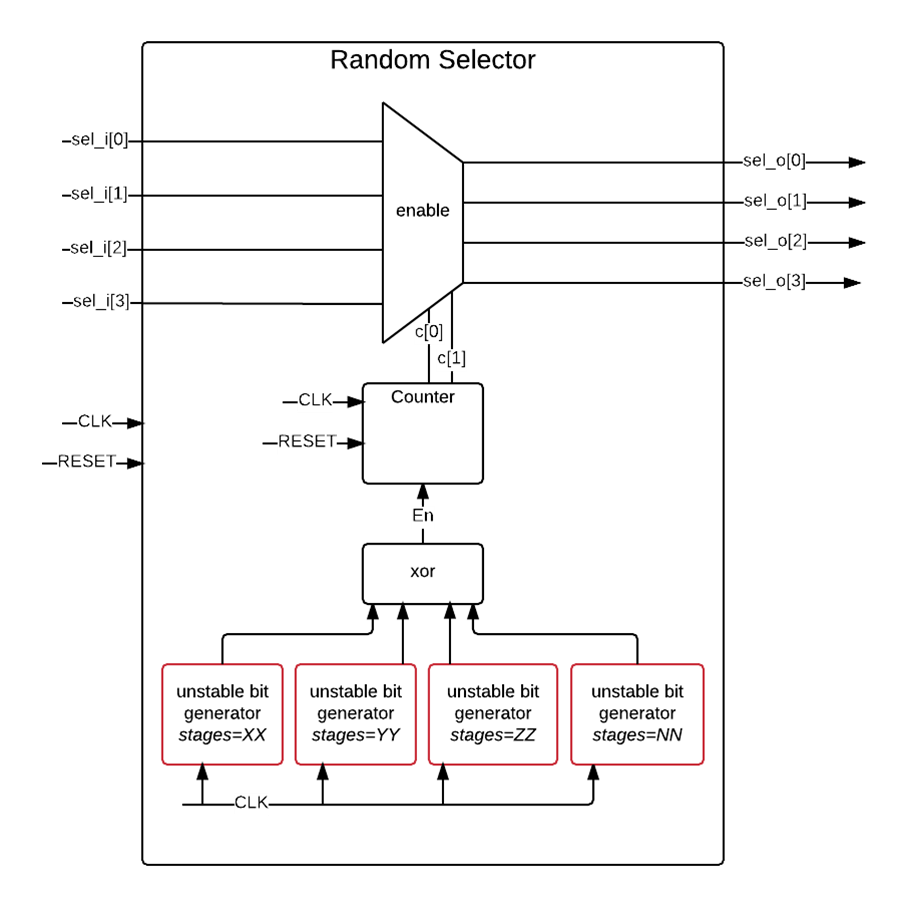
Fig. 49 True random number generator and arbitrator for singles mode
In the random selector, there are four instances of the unstable bit generator where each instance is a different stage. The outputs of the unstable bit generators are channelled through an XOR gate to add more randomness. The XOR output enables or disables a free running counter meaning if the XOR output is one, the counter increments, and if the XOR output is zero, the counter does not increment. In Fig. 49, the trapezoid labeled ‘enable’ is a multiplexor with a maximum of four inputs.
The output from the counter determines which input in the multiplexor is selected for output. For example, if there are four inputs to the multiplexor, the counter will select one of those four. If there are only two, the counter will select one of those two. More specifically, the counter’s maximum value is the least common multiple of the number of multiplexor inputs. The counter output is the modulo of the counter value and the number of inputs going into the multiplexor. For example, if there are four inputs, the LCM is 12 so this is the maximum value the counter can reach. If the counter output value is 11, the modulo of 4 and 11 is 3 which corresponds to selecting the fourth input (the inputs are numbered 0 to 3). This whole system is designed to create a fair selection of the inputs.
The following is a minimalistic example of a detector board function and design in singles mode. The detector board can have user-defined cores composed of modules that manipulates the data for a desired output. Fig. 50 provides an example module showing default inputs and outputs. The thick I/O markers are buses, and the thin I/O markers are single bits. More can be added. The detector board interface intelligently instantiates the correct number of user-defined cores based on the number of pipeline stages available. The data is handled by the interface without any user intervention.
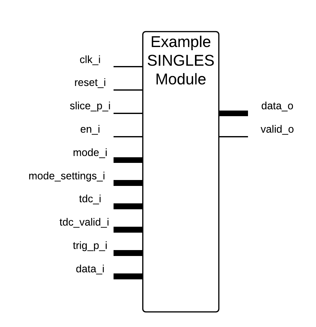
Fig. 50 Singles mode module example
Fig. 51 shows the state machine diagram for the example module above.
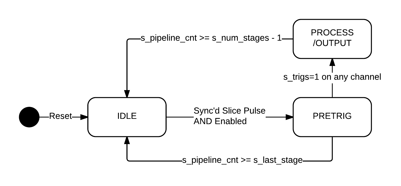
Fig. 51 Singles mode module state machine example
The detector board will enable each module within it sequentially to allow processing. Each module is initially in the IDLE stage where it waits for the conditions to move onto the PRETRIG stage. It must receive an enable signal from the detector board (en_i from Fig. 50) and the clock and slice must be ‘1’ or the high value simultaneously. Once in the PRETRIG stage, it waits for a triggered channel signal to move onto the PROCESS/OUTPUT stage. If there is no trigger received within the time set by the user in the singles mode settings (Fig. 53), it returns to IDLE. Also, once it is in the PROCESS/OUTPUT stage, it will return to IDLE after that same amount of user-defined time.
The following is a basic OpenPET example that computes the energy or area under the curve of the waveform. There is up to 16 data points utilizing 5 pipeline stages. Fig. 52 is an example of one of the word packs.
- 128-bit Word packs:
- 6-bit energies for 16 channels = 6*16 bits
- 9-bit address
- 4-bit hit trigger counter
- 4-bit packet ID for 4 packets = 4*4 bits
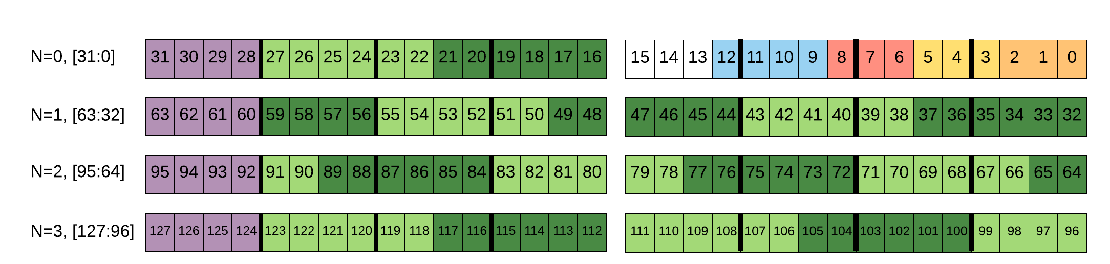
Fig. 52 Singles mode energy example word
For N = 0:
Starting from the least significant bit (LSB)
(2:0)   Detector board address (populated by parent)
(5:3)   DU address (populated by parent)
(8:6)   MB address (populated by parent)
(12:9)  Number of channels that triggered
(15:13) Not used
(21:16) Channel 0 energy
(27:22) Channel 1 energy
(31:28) Packet ID
As previously mentioned, the word is broken up into N number of 32-bit packets. For the rest of packets after N = 0, (27:0) contains channel energy and (31:28) is the packet ID. Each channel energy is 6 bits long as illustrated by the alternating green sections in Fig. 52 for N > 0. Also, some channels are split over different packets.
Fig. 53 shows the bit assignment for the singles mode settings for this example. This is set by Command ID: 0x0005.

Fig. 53 Singles mode settings for this energy example
Starting from the least significant bit (LSB)
(3:0)   Total number of ADC clock ticks to finish a single Event computation (2^4 = 16)
(7:4)   Reserved (max ADC clock ticks to process data: 2^8 = 256)
(15:8)  Reserved
(31:16) Not used
Note
- The event computation clock ticks should be greater than 1.
- The number of pipeline stages is predefined in the firmware as a constant.
- Pipeline Stages = ceil(Event Computation Clock Ticks/Slice Width) + 1, where ceil() rounds the number to the next highest integer.
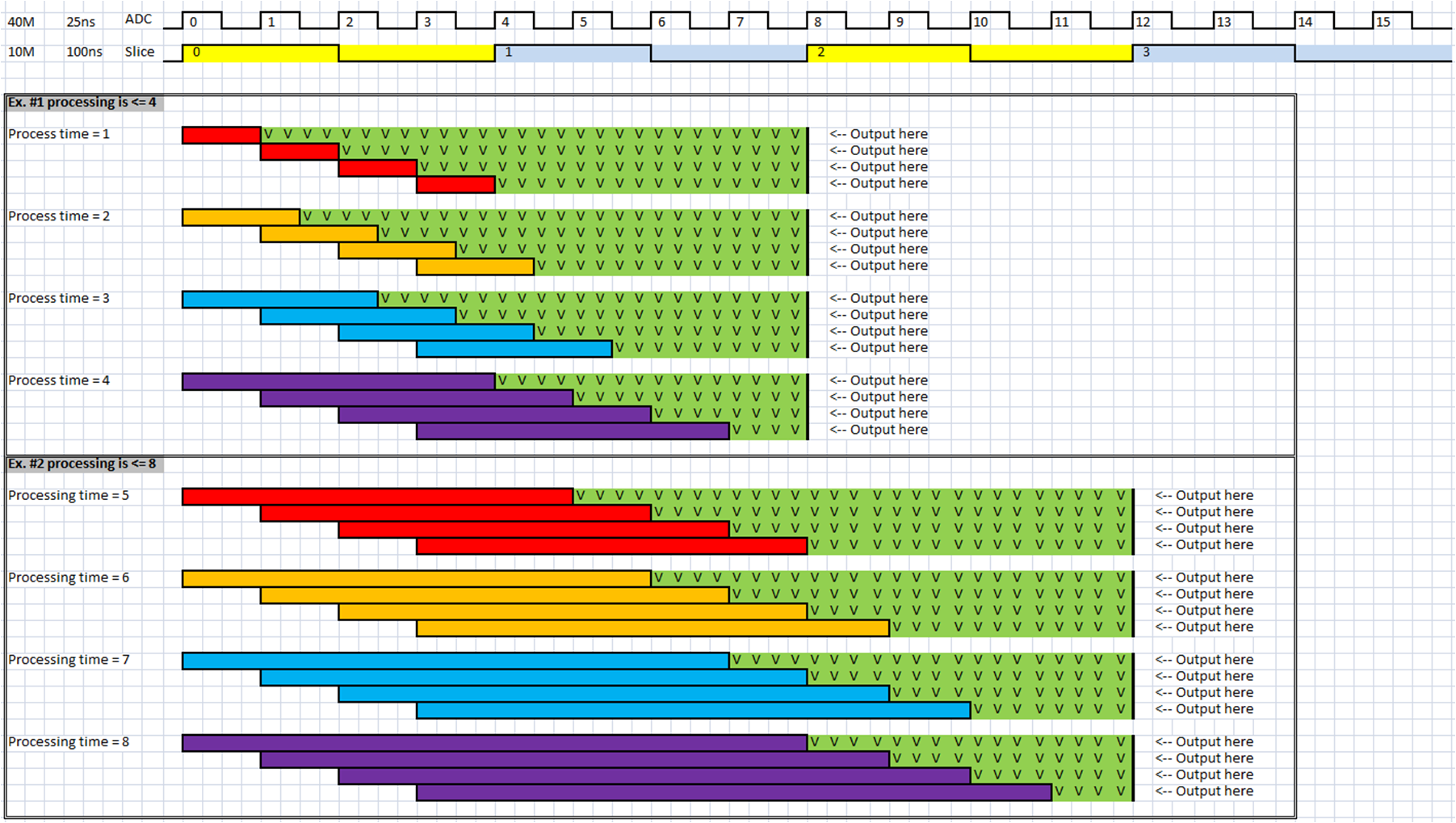
Fig. 54 Shows multiple examples of different processing ticks.
Since coincidence is important, OpenPET has a system of outputting data so that events that trigger in the same slice are processed and outputted in the same slice. In Fig. 54, there are eight examples divided into two sections. The top section shows when the processing time is 1 through 4 clock ticks (ADC domain), and the bottom section is for when the processing time is 5 through 8 clock ticks. The processing time is calculated by subtracting 1 from the maximum number of pipeline stages and multiplying the difference by N.
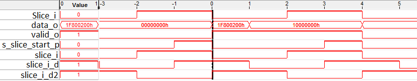
Fig. 55 Relationship beween valid_o and data_o at the DB level.
The timing of valid_o, data_o, and slice_i is shown in Fig. 55. In this simple example, the the valid_o encapsulates data_o. The length of valid_o depends on the slice width and algorithm implemented. The MSB of data_o’s first byte indicates that it is a Singles byte. The address is zero because the address gets populated by the parent i.e., the IO FPGA.
Serial Peripheral Interface
OpenPET utilizes a standard 32-bit wide Serial Peripheral Interface (SPI) to facilitate serial communications. The SPI structure is a master-slave architecture to connect the parent node to its children. Fig. 56 and Fig. 57 show the configurations of the master and slave SPIs. In the OpenPET system, the master SPI is on either the CUC or CDUC depending on the size of the system.
Fig. 56 Block diagram and specifications for the master SPI.
Currently, the master SPI is configured to have ten slaves - two for the IO FPGAs and eight for either the DUCs or DBs. For example, if the system is small, the master SPI would be on the CDUC with two slaves for the IO FPGAs and eight slaves, one for each detector board. However, for a standard system, the master SPI is on the CUC with two slaves for the IO FPGAs and eight slaves, one for each DUC.
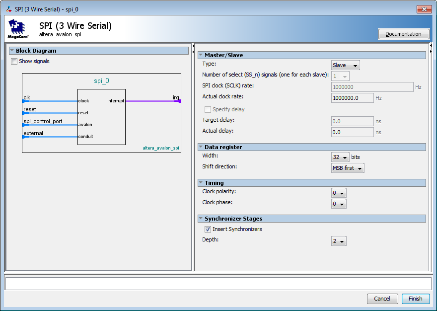
Fig. 57 Block diagram and specifications for the slave SPI.
The DUC Support Board is a special case having a slave SPI as well as a master. Commands from a CUC (master SPI) flow to the slave SPI on the DUC. If the command destination is a detector board, the command then continues to the master SPI on the DUC to the slave SPI on the detector board. The master-to-slave SPI transition on the DUC is invisible to the user. The detector boards only have slave SPIs.
Fig. 58 gives an example waveform of a 32-bit SPI with broadcasting.
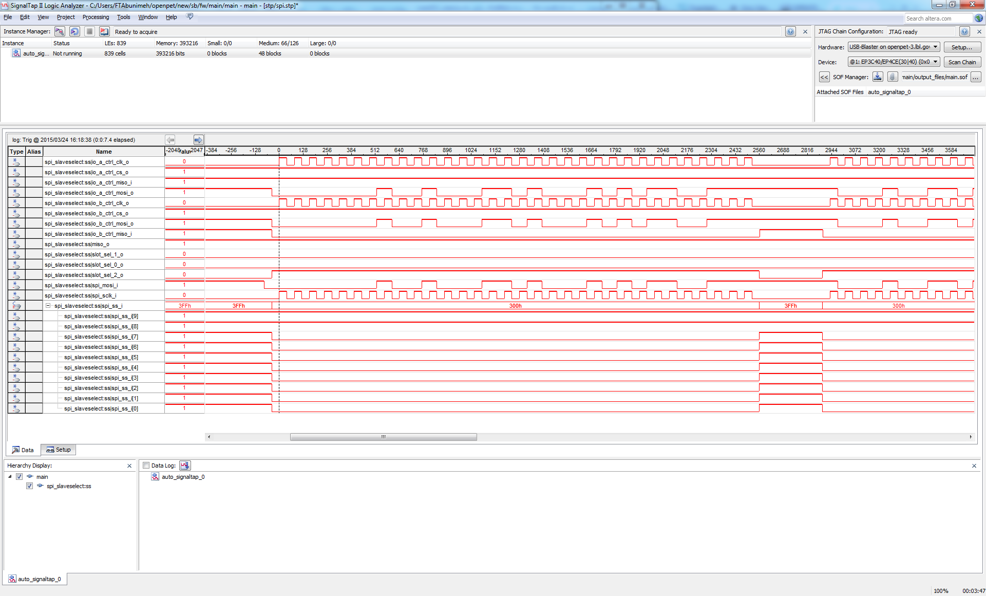
Fig. 58 Example waveform of a standard 32-bit SPI with the broadcasting flag set to 1.
Fig. 59 shows the logic each SPI follows when receiving a command.
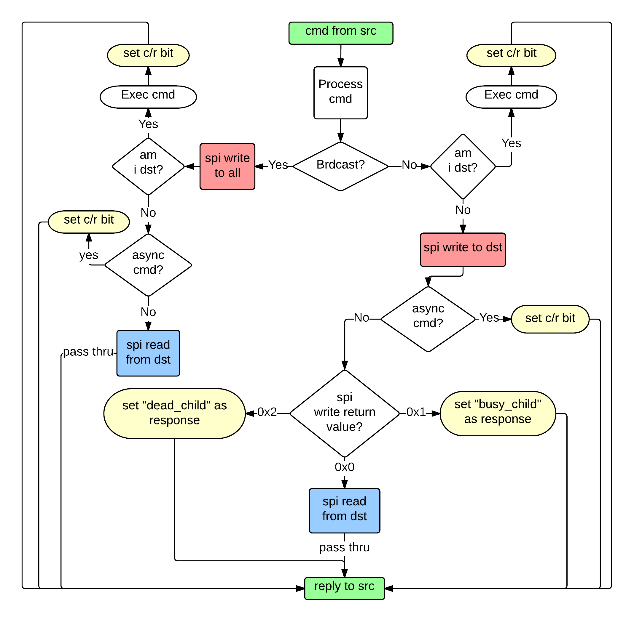
Fig. 59 Flowchart depicting the command flow logic
A command originates from a source, usually the Host PC, and consists of the command ID, source address, destination address, and the payload. The commands are constructed using the little-endian format. The master SPI on the parent node (e.g. CUC or CDUC) receives the command from the Host PC. It then processes the command and determines if the broadcasting flag is set to 1. If so, it will pass the command down to all its children and the response it receives will be from the child specified in the destination address. Additionally, if the CUC or CDUC flag is set to 1, the parent will execute the command itself and the reply will be from the parent instead of the child specified in the destination address.
After it determines the status of the broadcasting flag and performs any necessary actions, it will check the destination of the command. As mentioned in the previous paragraph, if itself is the destination, it will execute the command and reply to the source. If it is not the destination, it will write the command to the specified destination (if the broadcasting flag was not set to 1) and determine if the command is asynchronous. If it is, the C/R bit is set to 1, and the parent does not keep polling for a response. It simply sends the command. If the command is not asynchronous, the parent keeps reading until it receives a valid response from the child and performs the corresponding action.
When a command is passed from a parent node to a child node, it follows the steps listed in Fig. 60.
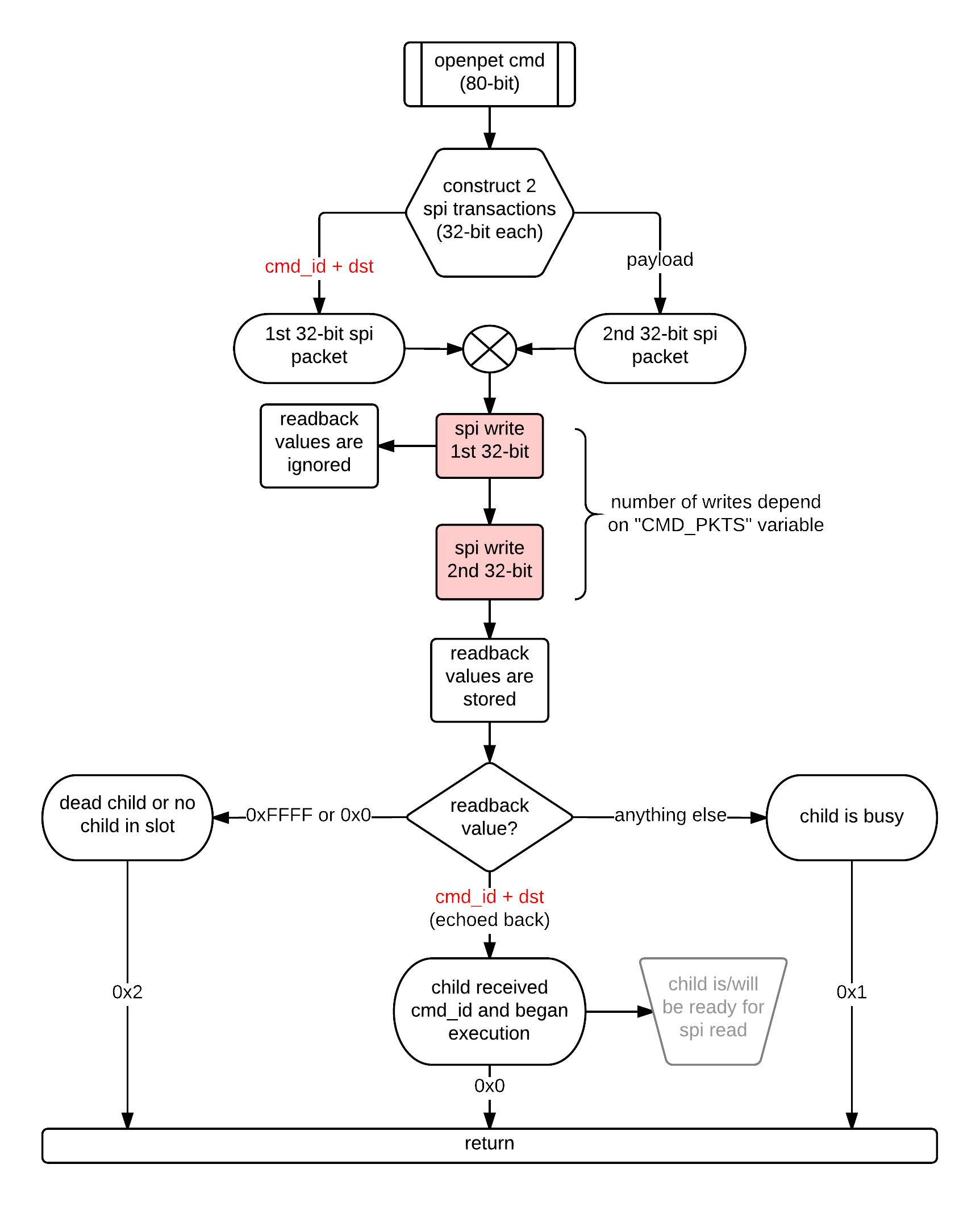
Fig. 60 SPI write command flowchart
When reading a response from the destination, it follows Fig. 61.
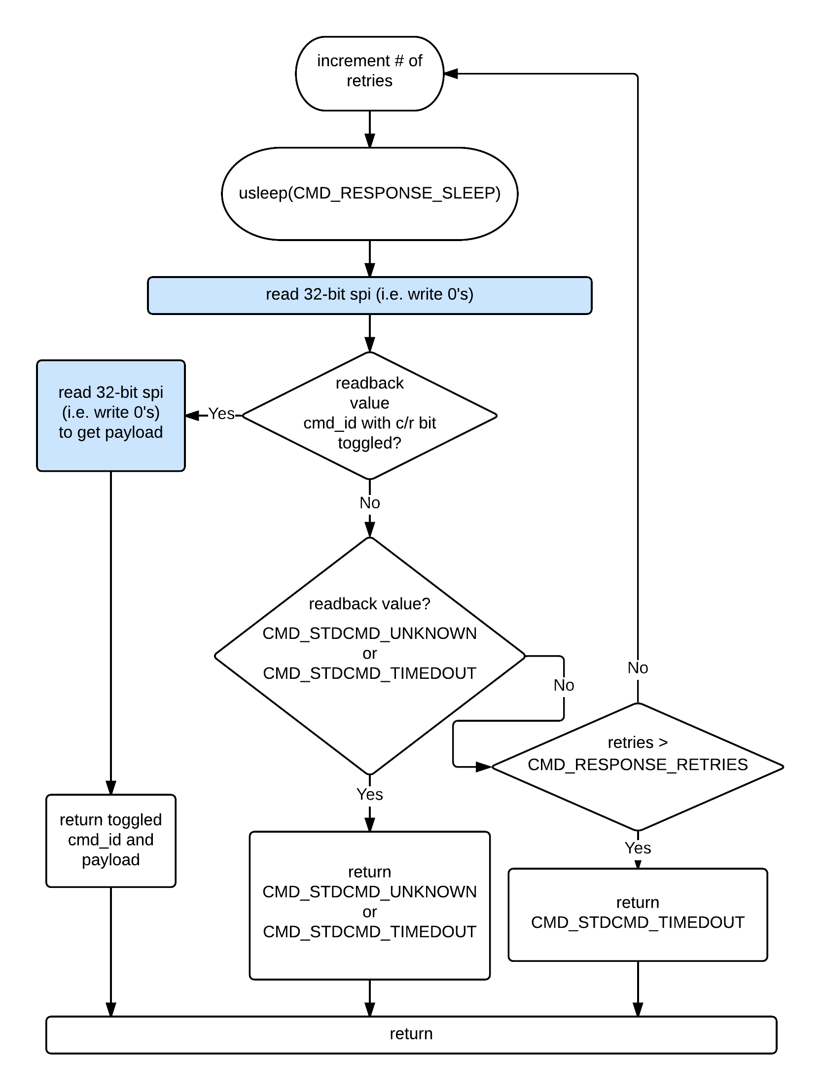
Fig. 61 SPI read command flowchart
Example
The following is an example of SPI communications between nodes. In this case, the parent node is the Host PC, the child node is the CUC or CDUC, and the grand child is the detector board.
- The Host PC constructs a command:
cmd = 1 (PING)src = 0x4000 - Host PC addressdst = 0x0003 - DB in slot 3payload = 0x0000ABCD
- Using QUSB, the Host PC writes that command to the first node, e.g., CUC or CDUC. It can communicate through any medium (ethernet, USB, fiber optic).
- The Host PC will keep reading for a valid response from the child until the number of retries (“CMD_READ_RETRIES”) is reached. Between each trial, a time period of “CMD_READ_RETRIES_TIME” is observed. CMD_READ_RETRIES and CMD_READ_RETRIES_TIME are constants defined in the software running on the Host PC.
- There are five possible responses:
- If the command ID is equal to the command ID sent, i.e. C/R flag is still 0 and not 1, then the child is out of memory. (when not in async/nonblocking calls)
- If the command ID is equal to “CMD_STDCMD_UNKNOWN”, then the child doesn’t understand this command.
- If the command ID is equal to “CMD_STDCMD_TIMEDOUT”, then the grandchild timed out.
- If the command ID is equal to “CMD_STDCMD_DEADCHILD”, then the grandchild is dead or doesn’t exist. Also, if the Host PC number of retries >= CMD_READ_RETRIES, then the child is presumed dead.
- If the command ID is equal to “CMD_STDCMD_BUSYCHILD”, then the grandchild is busy executing the previous command.
- Once a child (CUC or CDUC) receives a command from HostPC, the following can occur:
- If broadcast flag is set, the parent will pass the command down to all its children. The response will be from the child specified in destination address.
- If the command destination is the CUC or CDUC (itself), it will be executed locally and returned with the proper response flag and payload. The reply will be from that unit and not from the child specified in destination address.
- If the command is passed down (WRITE) to the grandchildren, the commands are modified into two 32-bit SPI transactions. The first transaction is 32-bits and contains the “C/R ID” (16 bits) + “DST address” (16 bits). The second contains the payload.
- If grand child doesn’t respond to WRITE, it doesn’t exist or is dead, i.e. CMD_STDCMD_DEADCHILD is returned to parent.
- Child will be polling (READ) grandchild for “CMD_RESPONSE_RETRIES” times with CMD_RESPONSE_SLEEP time period in between. CMD_RESPONSE_RETRIES and CMD_RESPONSE_SLEEP are defined in child’s embedded software i.e. cmd.h
- If the number of retries >= CMD_RESPONSE_RETRIES, then CMD_STDCMD_TIMEDOUT is sent back to parent. (as described in 4. C)
- (1st 32-bit SPI transaction) If child receives CMD_STDCMD_TIMEDOUT or CMD_STDCMD_UNKNOWN from a grandchild, it will just pass them back to parent. There will be NO second transaction.
- If child receives correct response with proper response flag set, then the child performs one more transaction to READ the payload from the grandchild. Once the payload is received, a response to parent will be constructed and ready to be READ/polled by parent.
- If while WRITING to a grandchild, the grandchild is still performing a task, the child will send back CMD_STDCMD_BUSYCHILD to parent. Because the child will be expecting the same command echoed back, if a different command is echoed back, then the grandchild is still working on the previous command.
Fig. 62 shows the debugging screen of sending a ping command (ID = 1) to a detector board. The first line beginning with [0] shows the command received which is broken down into its components in the next four lines. The command source is 0x4000 which is the Host PC, and the destination is Detector Board 3. The payload for this command is meaningless since it is merely a ‘ping’. The slave SPI is then selected. The WRITING value (first [SPI] line) breaks down into 0x00010003 which is the command ID combined with the destination address and the payload 0x0000ABCD. Each is a 32-bit SPI transaction. Once the correct CMD ID and destination are read back ([SPI] line three), the command is executed. The master SPI then reads from the slave for the CMD ID and destination with the C/R bit set to 1 ([SPI] line four). After that, it reads the payload back. At this point, the command is complete, and a response is generated and sent back to the Host PC (final line).
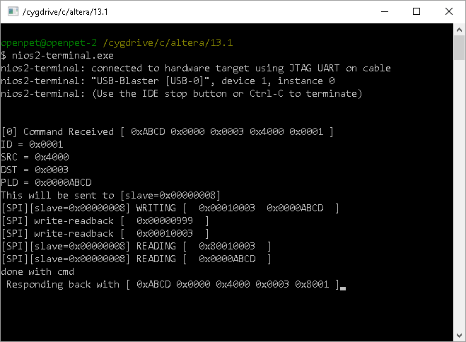
Fig. 62 Example of a command successfully executed with Detector Board 3.
The following screen shot (Fig. 63) shows the result of unsuccessfully sending a command to a detector board. Since the write-readback value is 0xF, there is a broken or non-existent detector board in that slot. Therefore, the corresponding response is generated (last line).
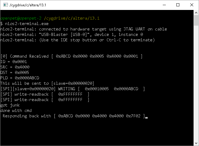
Fig. 63 Example of a command sent to a non-existent detector board.
List Mode Data
(Use combination of User Guide section 2.5.1 and Framework section 3.)
Introduction
(Expand on Framework section 3.1.)
Event Words
(Include single event mode and coincidence event mode. See Framework section 3.2.)
Status Words
(See Framework section 3.3.)
Coding and Decoding List Mode Data(?)
(See Framework section 3.4.)
Bootup Sequence
This bootup sequence describes the steps of the OpenPET system after the user has programmed the EPCS. It begins when the system powers on and ends with the detector boards waiting for the first SPI command. The basic steps can be explained through a small system example.
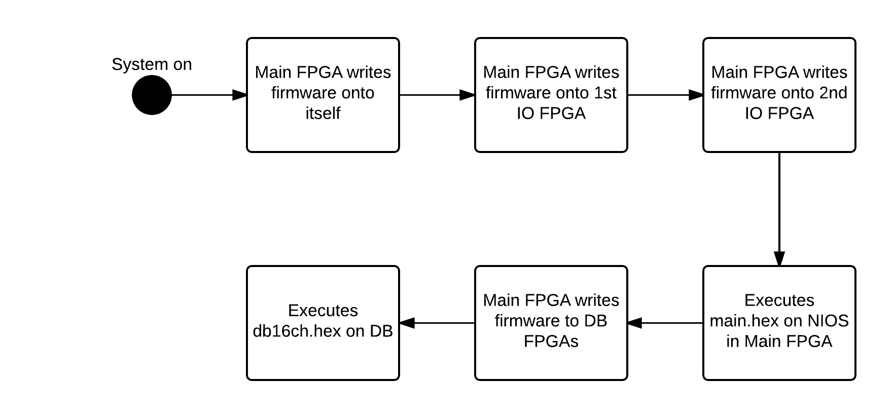
Fig. 64 Diagram of the bootup sequence for a small OpenPET system
In a small system, there is a single support board that connects to all the detector boards (Fig. 41). The basic sequence of steps is outlined in Fig. 64. On the support board is the EPCS chip that is used to configure all the FPGAs on the support board and detector boards. The table below and Fig. 65 show the structure of the EPCS. The table outlines the basic block locations. The blocks are further explained in Fig. 65.
| Block | Start Address | End Address |
|---|---|---|
| Page_0 | 0x00000000 | 0x00368E43 |
| main.hex | 0x00368E44 | 0x0037A13B |
Note
- The detector board images are deliberately written to a different location (0x00400000)
- All the addresses in this file are byte addresses
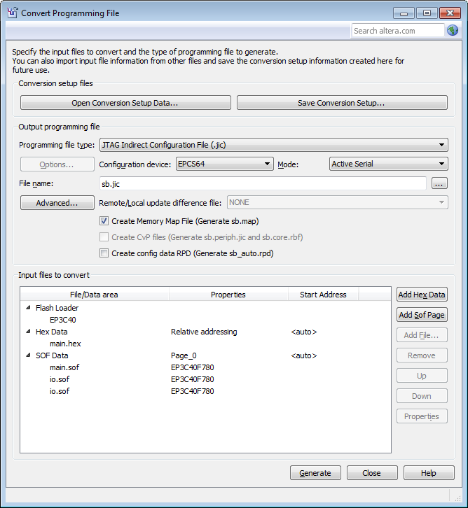
Fig. 65 EPCS hierarchy
Using the Altera boot loader, the Main FPGA configures itself first with the firmware from the EPCS. Next, it configures the IO FPGAs one at a time with different but identical firmware. In other words, there are two IO FPGA firmware blocks on the EPCS, and each gets loaded onto an IO FPGA (see Fig. 65). The IO sof contains the bitstream and an elf executable. Once the firmware is loaded onto the IO FPGA, the elf program is run. This program initializes and resets the IO FPGA and then idles as it waits for an SPI command from the user.
After the Main FPGA loads the firmware onto the IO FPGAs, it copies the main.hex program over to itself and executes it on NIOS. This program does multiple things. It initializes the Ethernet, initializes the current node (CDUC in this case), performs a soft reset, and then programs the detector boards. To program the detector boards, the Main FPGA uses what is called Active Serial Configuration which means the FPGA is the master device and the EPCS is the slave device. The Main FPGA accesses the EPCS to get the detector board images (see note above) and then programs all the detector boards simultaneously. The sof of the detector board includes the bit stream with an elf executable. The detector board FPGA runs the elf program which performs a reset and then waits for an SPI command. At this point the system is waiting for the user to tell it to do something. This concludes the bootup sequence.
System Reset
There are three different types of system resets possible.
The first is a hard reset that resets the entire system. This is the top level reset method. There is a button on either the support board or the Host PC board that will shut down any and all FPGAs running.
The second method is a firmware reset. This keeps the FPGAs running but essentially shuts down the system clock signal so the system still cannot do anything. It unlocks the PLL so that no clock signal can be outputted. When the PLL is locked, a clean system clock signal can be transmitted throughout the system. However, if the PLL is not locked, then no system clock signal can be sent through the system.
The third reset is the soft reset mentioned in the Bootup Sequence above. In this case, there is no physical button to press, and the PLLs are locked. This reset affects the QuickUSB and any firmware or software communication blocks. It takes about 10ms on bootup.